HBM4 Cut to 9.6 Gbps and NVLink 6 Trimmed to 3 TB/s: Why NVIDIA Lowered Its Vera Rubin Spec Targets
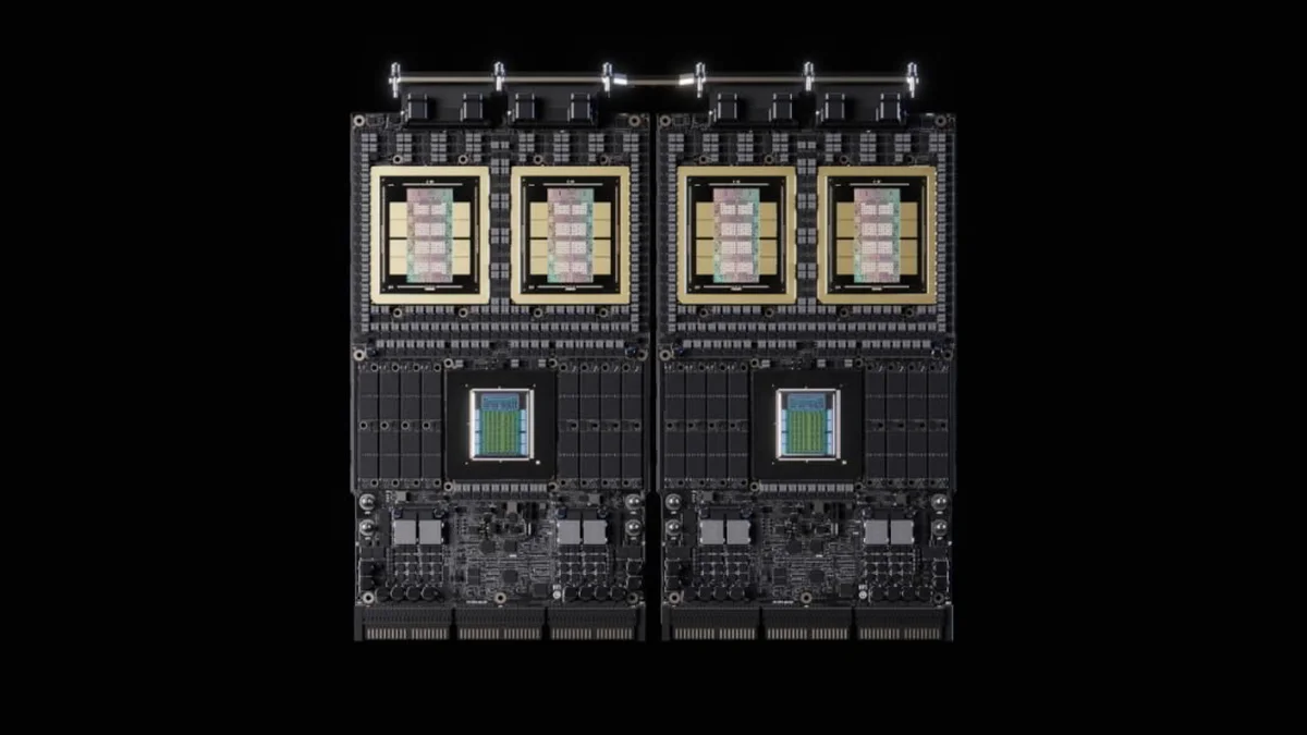
NVIDIA has quietly updated the official technical specification sheets for its next-generation Vera Rubin architecture, revising target bandwidth figures downward across both memory and rack-scale interconnects. According to the updated platform documentation, per-pin speeds for HBM4 memory have been reduced from 11.7 Gbps down to 9.6 Gbps, while sixth-generation NVLink 6 bidirectional throughput per GPU has moved from 3.6 TB/s to 3.0 TB/s.
From 1,580 TB/s to 1,400 TB/s: Inside the HBM4 9.6 Gbps Per-Pin Revision
The first major adjustment targets the memory subsystem surrounding each Rubin GPU. While preliminary roadmap documentation projected HBM4 stacks operating at an aggressive 11.7 Gbps per pin (well above the base 8 Gbps JEDEC HBM4 specification), NVIDIA's updated product datasheet scales that operating clock back to 9.6 Gbps per pin, representing an 17.9% drop in per-pin data rate.
While individual Rubin GPUs retain their full 288 GB HBM4 capacity across eight memory stacks, the lower pin speed directly reduces aggregate memory bandwidth across every system tier:
- Individual Rubin GPU (288 GB HBM4): Memory bandwidth moves from 22 TB/s down to 19.25 TB/s.
- NVIDIA Vera Rubin Superchip (2 Rubin GPUs + 1 Vera CPU, 576 GB HBM4): Aggregate memory bandwidth shifts from 44 TB/s down to 38.5 TB/s (-12.5%).
- NVIDIA Vera Rubin NVL4 Module (4 Rubin GPUs + 2 Vera CPUs, 1.1 TB HBM4): Listed memory bandwidth now stands at 77 TB/s.
- NVIDIA Vera Rubin NVL72 Rack (72 Rubin GPUs + 36 Vera CPUs, 20.7 TB HBM4): Total rack-level memory bandwidth drops from 1,580 TB/s down to 1,400 TB/s (-11.4%).
- HGX Rubin NVL8 Baseboard (8 GPUs): Specifications step down from 2.3 TB capacity and 176 TB/s bandwidth to 2 TB and 130 TB/s.
NVLink 6 Signal Integrity: Why NVIDIA Tuned the Nyquist Frequency from 56 GHz to 47 GHz
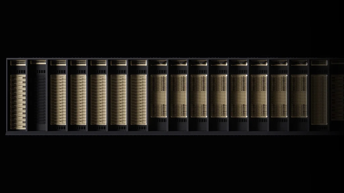
Alongside the memory revision, NVIDIA adjusted its sixth-generation NVLink 6 interconnect targets. Unidirectional NVLink bandwidth per GPU was trimmed from 1.8 TB/s to 1.5 TB/s, bringing peak bidirectional GPU bandwidth down from 3.6 TB/s to 3.0 TB/s (-16.7%). At the module level, the Vera Rubin Superchip moves from 7.2 TB/s to 6.0 TB/s (with the 4-GPU NVL4 module rated at 12 TB/s), HGX NVL8 switch fabric shifts from 28.8 TB/s to 24 TB/s, and total scale-up bandwidth across a full Vera Rubin NVL72 rack settles at 216 TB/s instead of 260 TB/s. Meanwhile, the coherent NVLink-C2C link between the 88-core custom Vera Olympus CPU and the Rubin GPUs remains untouched at 1.8 TB/s per Superchip (65 TB/s per NVL72 rack).
The engineering driver behind this adjustment is electrical signal integrity: NVIDIA lowered the NVLink Nyquist frequency target from 56 GHz to 47 GHz. Reducing the Nyquist frequency relaxes the extreme electrical tolerances required across high-speed SerDes transceivers, dense printed circuit boards, copper backplane cabling, and advanced packaging substrates. That packaging bottleneck is already at the center of the $5 billion investment wave from NVIDIA, AMD, and Intel into Taiwanese ABF substrate factories to secure multi-layer chip carriers through the end of the decade.
| System Metric | Vera Rubin NVL72 (Previous Target) | Vera Rubin NVL72 (Updated Spec) | Vera Rubin Superchip (Updated Spec) |
|---|---|---|---|
| Compute Configuration | 72 Rubin GPUs | 36 Vera CPUs | 72 Rubin GPUs | 36 Vera CPUs | 2 Rubin GPUs | 1 Vera CPU (88 Olympus cores) |
| HBM4 Speed Per Pin | 11.7 Gbps | 9.6 Gbps | 9.6 Gbps |
| HBM4 Capacity & Bandwidth | 20.7 TB | 1,580 TB/s | 20.7 TB | 1,400 TB/s | 576 GB | 38.5 TB/s (down from 44 TB/s) |
| NVLink 6 Bandwidth | 260 TB/s (3.6 TB/s per GPU) | 216 TB/s (3.0 TB/s per GPU) | 6.0 TB/s (down from 7.2 TB/s) |
| NVLink-C2C CPU-GPU Bandwidth | 65 TB/s | 65 TB/s | 1.8 TB/s |
| NVFP4 Inference / FP32 Compute | 3,600 PFLOPS / 9,360 TFLOPS | 3,600 PFLOPS / 9,360 TFLOPS | 100 PFLOPS / 260 TFLOPS |
| Rack Power Envelopes | Not specified | MaxP: 227 kW | MaxQ: 187 kW | MaxLPS: 156 kW | Liquid-cooled (45°C inlet temperature) |
Unchanged Compute FLOPS, 227 kW Power Profiles, and What It Means for GeForce RTX Gamers
Crucially, raw shader and Tensor Core compute figures remain completely intact. A full Vera Rubin NVL72 rack still delivers 3,600 PFLOPS of NVFP4 inference (50 PFLOPS per GPU), 2,520 PFLOPS of NVFP4 training, 1,260 PFLOPS of FP8/FP6 compute, 9,360 TFLOPS of FP32, and 2,400 TFLOPS of native FP64 performance. The updated specification sheet also formalizes three rack power envelopes operating at a 45°C liquid cooling inlet temperature: MaxP at 227 kW, MaxQ at 187 kW, and MaxLPS at 156 kW, while paving the way for NVIDIA's optical Rubin Ultra NVL576 architecture further down the roadmap.
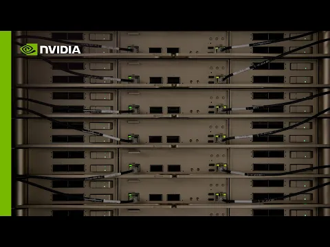
For PC gamers, NVIDIA's willingness to trade roughly 11% to 17% of peak theoretical memory and interconnect bandwidth for better signal integrity carries direct supply chain implications. Easing electrical stress across TSMC N3P silicon dies and CoWoS-L interposers directly improves manufacturing yields, reducing wafer scrap rates at a time when high-end gaming GPUs built on GDDR7 memory compete for advanced foundry allocation.
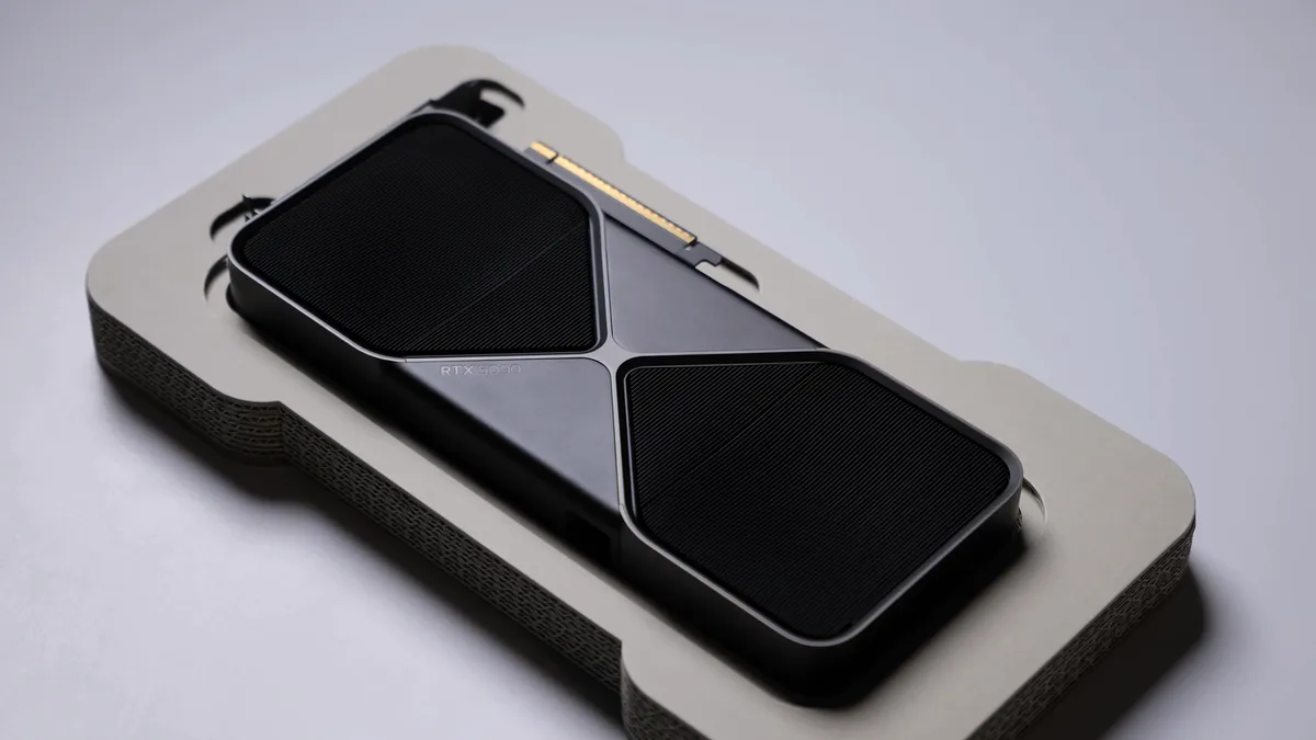
NVIDIA GeForce RTX 5090 Graphics Card (32GB GDDR7, Blackwell Architecture)
My Test Bench
Looking at these revised numbers from my test bench perspective, NVIDIA's engineering trade-off makes complete sense for volume manufacturing. Driving eight 2048-bit HBM4 stacks per GPU at 11.7 Gbps per pin while simultaneously pushing passive copper backplanes at a 56 GHz Nyquist frequency leaves almost zero electrical margin across a 227 kW rack of 1,296 chips. Scaling back to 9.6 Gbps on HBM4 and 47 GHz on NVLink 6 guarantees rock-solid rack stability and higher silicon yields without sacrificing a single FLOP of compute, keeping wafer supply healthier for both data centers and future consumer GeForce architectures.
Check Availability for NVIDIA GeForce RTX 5080 on Amazon→

PC hardware enthusiast and competitive gamer, Arthur 'Heimdall' splits his time between France and the UK working in enterprise B2B software solutions. A business school graduate passionate about component benchmarking, he has been building, modding, and tuning PCs since childhood, optimizing every thermal degree and millisecond of display latency. An avid gamer across Assassin's Creed and sandbox titles, he forged his alliance with Grimtag and Chaya during late-night World of Warcraft raids before joining Pro-Gamer.