9,600 MT/s LPDDR5X and 4F² Vertical Transistors: How YMTC Is Taking On the DRAM Triopoly Without EUV
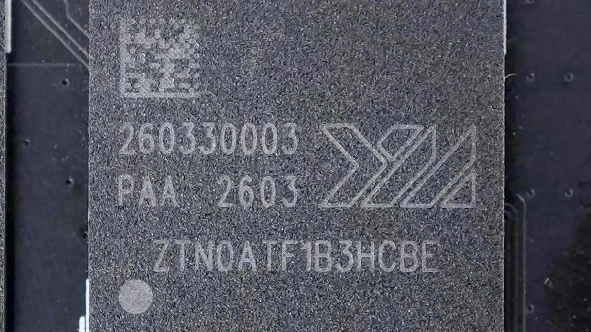
Best known among PC builders for the 3D NAND flash memory chips powering many budget-friendly NVMe SSDs, Chinese semiconductor manufacturer YMTC (Yangtze Memory Technologies Corp) is now making a major play in the tightly guarded DRAM market. According to industry data from Counterpoint Research, the Wuhan-based company is preparing to start high-volume mass production of 9,600 MT/s LPDDR5X memory at its Fab 3 facility, following a full year of quiet initial manufacturing on its first-generation lines.
From 5,000 Secret Monthly Wafers at Fab 2 to 9,600 MT/s Mass Production at Fab 3
While industry observers have known for some time that YMTC intended to expand beyond NAND flash into DRAM manufacturing, the actual scale of its existing operations had remained largely under wraps. Counterpoint Research reveals that YMTC has already been producing roughly 5,000 wafers per month of 16 Gb LPDDR5X DRAM (2 GB per die) running at 7,500 MT/s at its Fab 2 plant since October 2025, without relying on High-k Metal Gate (HKMG) processes for that initial iteration.
That pilot run laid the foundation for a full-scale commercial push at Fab 3. By targeting data transfer speeds of 9,600 MT/s, YMTC's next-generation LPDDR5X goes head-to-head with the fastest low-power memory modules from Samsung, SK Hynix, and Micron. For gamers, the timing is critical: at a moment when surging RAM and SSD component costs are squeezing sub-$1,000 gaming laptops and handheld gaming PCs rely entirely on fast LPDDR5X bandwidth to feed their integrated GPUs without dedicated VRAM, the arrival of another major supplier alongside domestic rival CXMT could bring welcome relief to hardware OEMs.
4F² Vertical Channel Transistors and Xtacking 4.0: Taking the Opposite Path From Micron
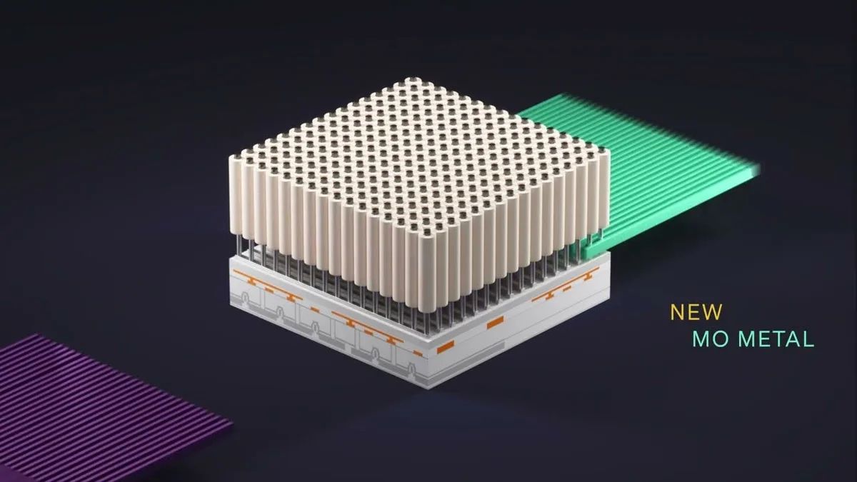
Cut off from extreme ultraviolet (EUV) lithography scanners due to US export controls and restricted to deep ultraviolet (DUV) tools, YMTC is compensating for optical scaling limits through cell geometry and 3D packaging. Its 9,600 MT/s LPDDR5X chips at Fab 3 utilize a 4F² memory cell layout paired with Vertical Channel Transistors (VCT), shrinking each cell's theoretical footprint by about one-third compared with the conventional 6F² structure used in mainstream DRAM today.
Crucially, YMTC is also bringing its signature 3D NAND weapon to DRAM manufacturing: Xtacking 4.0. Using wafer-to-wafer hybrid bonding, YMTC processes the memory cell array on one silicon wafer and the peripheral CMOS logic circuits on a separate wafer, then permanently fuses the two together face-to-face via microscopic embedded metal bumps.
This architectural gamble stands in sharp contrast to the strategy outlined on October 21 by Scott DeBoer, Micron's President and Chief Technology and Products Officer, right as Micron prepares its upcoming 1-delta DDR6 and LPDDR6 memory roadmap for 2027. After two decades of internal research into 4F² DRAM, Micron decided to walk away from the design, arguing that real-world density remains bottlenecked by capacitor spacing and opting instead to keep scaling 6F² across its 1-delta and 1-epsilon nodes until true 3D DRAM is economically viable. By contrast, YMTC and CXMT are pushing aggressively into 4F² right now, while YMTC's mastery of Xtacking 4.0 (and a potential future Xtacking 5.0 iteration) already gives it a foundational advantage for the eventual transition to full 3D DRAM.
My Test Bench: Why YMTC's DRAM Push Is Great News for Handheld Gaming APUs
Whenever I benchmark the latest Windows and SteamOS gaming handhelds or ultrabooks powered by RDNA 3.5 integrated graphics, the bottleneck is always the same: LPDDR5X memory speed dictates your 1080p frame rate ceiling, while DRAM contract pricing dictates whether a device stays affordable. Watching YMTC push its own LPDDR5X dies to 9,600 MT/s without EUV lithography by repurposing its Xtacking 4.0 hybrid bonding reminds me of how quickly the company disrupted the PCIe 4.0 NVMe SSD market three years ago. If Fab 3 yields scale smoothly across 2026 and 2027, having an aggressive new contender challenging the traditional DRAM triopoly is our best shot at seeing 24 GB and 32 GB handhelds become standard without crossing the $1,000 mark.

PC hardware enthusiast and competitive gamer, Arthur 'Heimdall' splits his time between France and the UK working in enterprise B2B software solutions. A business school graduate passionate about component benchmarking, he has been building, modding, and tuning PCs since childhood, optimizing every thermal degree and millisecond of display latency. An avid gamer across Assassin's Creed and sandbox titles, he forged his alliance with Grimtag and Chaya during late-night World of Warcraft raids before joining Pro-Gamer.