Just a Few Percent Behind TSMC and Betting on 14A High-NA EUV: Why Intel Says the Next CPU Battle Comes Down to Scale
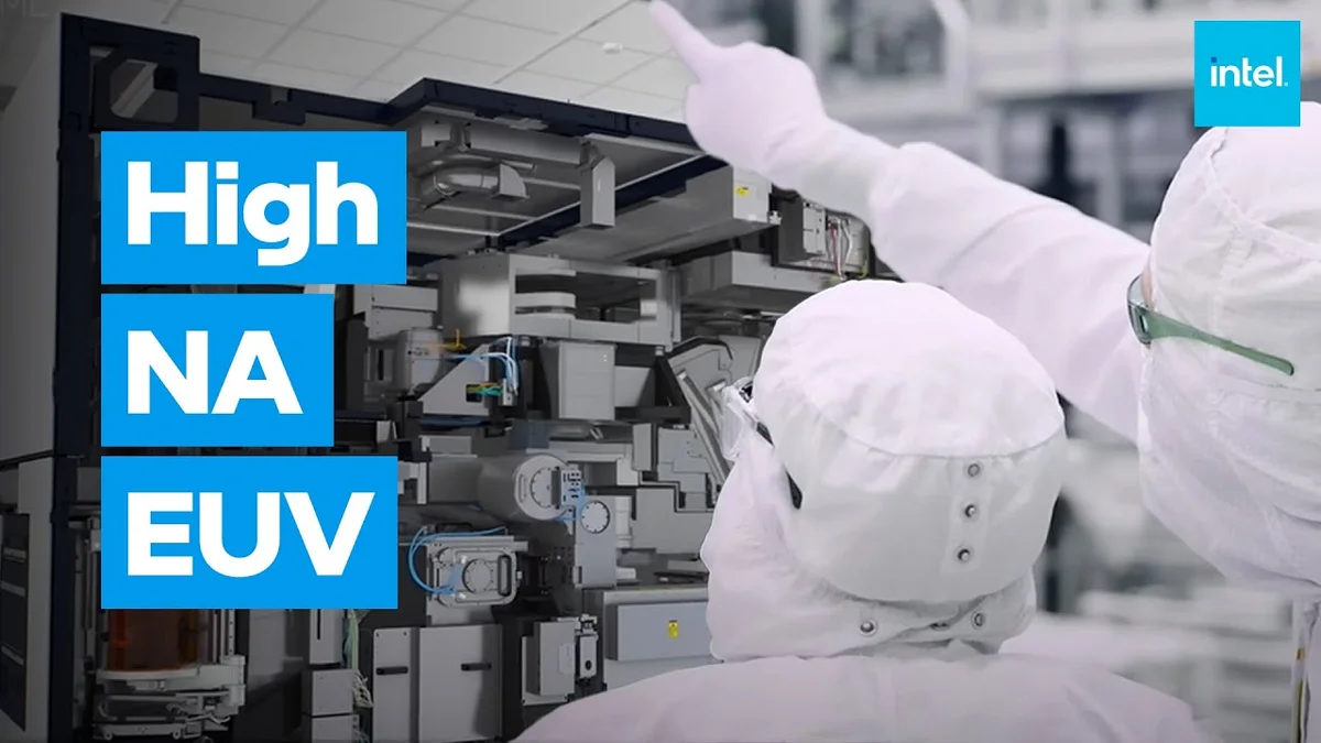
Where does Intel Foundry truly stand against TSMC's manufacturing dominance as the next wave of desktop and mobile PC processors takes shape? During an extensive two-day tour inside Intel's most advanced Oregon research labs and fabrication facilities on the Dwarkesh Podcast, the company's top silicon engineers laid out a candid assessment. According to Intel Chief Technology Officer (CTO) Pushkar Ranade and Vice President and General Manager of Manufacturing Development and Customer Engagement Chris Auth, the historic multi-generation transistor gap is over: competing with the Taiwanese foundry giant now comes down to wafer scale, yield consistency, and the architectural pairing of backside power delivery with High-NA EUV lithography.
Technology vs. Wafer Scale: Why Closing a Few Percent of PPA Matters Less Than Execution
For nearly a decade following Intel's troubled 10nm transition, semiconductor rivalries were framed around which foundry held an absolute lead in transistor density. According to Pushkar Ranade, benchmarking one foundry as strictly ahead or behind only makes sense when a manufacturer is a full generation behind. From a pure technology standpoint, Intel's CTO asserts that the company is "already there" with its modern process nodes.
While Ranade acknowledges that Intel's nodes might still sit "maybe a few percent off on performance or power or area density" compared to TSMC, he argues that tiny theoretical margins are no longer the deciding factor for major silicon customers: "You can be off by a few percent, but you need to be on time. Your execution needs to be such that your yields are very high to support very large and very rapid ramps. So that actually is more important than catching up on a few percent on performance or area."
At the same time, Ranade openly admits that TSMC remains "a much larger wafer manufacturer today than we are," noting that catching up in sheer manufacturing scale will be "a slow process, and a gradual process." That challenge is compounded by a hard physical ceiling across the global supply chain: even with unlimited capital, the semiconductor industry could realistically only double (2x) its leading-edge output in the near term, as Dutch lithography leader ASML produces fewer than 100 EUV systems per year.
High-NA EUV Meets Backside Power: How Intel 14A Avoids TSMC's Double Patterning
The sharpest technical divergence between the two chipmakers revolves around ASML's next-generation High-NA EUV lithography machines. By boosting optical resolution on the silicon wafer to print features with a pitch (the center-to-center distance between two lines) between 16 nanometers and 8 nanometers in a single exposure, High-NA EUV allows foundries to avoid complex multi-stage printing. While Intel moved aggressively to install the first High-NA EUV tools in Oregon, TSMC has opted to stick with conventional Low-NA EUV and multi-patterning on its immediate nodes.
According to Chris Auth, Intel is uniquely positioned to make High-NA EUV work economically and technically on its upcoming 14A process because of backside power delivery (PowerVia). By moving the entire power delivery network to the underside of the silicon wafer, Intel frees up critical routing space on the front side where computing transistors and data interconnects reside.
"We use backside power, that means that you actually alleviate some of the pitch requirements you have on the front side. And that allows you to print that directly with High-NA," Auth explained. "TSMC has to run very tighter pitches because they don't have backside power, and they can't do that with High-NA, so they have to use double patterning EUV." Because looser front-side pitches provide a wider error tolerance, Intel can print critical layers in a single High-NA pass. Auth also confirmed that Intel 14A is already available as an active option in the foundry's Process Design Kit (PDK) today, handled on a customer-by-customer basis.
From Panther Lake and Nova Lake to Stacked Transistors: What It Means for PC Gamers
For PC gamers and hardware enthusiasts, this manufacturing battle directly shapes the upcoming Core Ultra roadmap. While Intel 18A brings RibbonFET Gate-All-Around transistors and PowerVia backside power to volume production with Panther Lake, Intel is taking a pragmatic dual-sourcing approach for its next flagship gaming lineups: as seen in the 28-core Intel Core Ultra 9 4995HX "Nova Lake-HX" flagship specifications and the first desktop Nova Lake-S motherboards built around the LGA 1954 socket, Intel is blending internal tiles with TSMC 2nm silicon while preparing 14A for the next architectural leap.
Looking beyond 14A toward sub-nanometer nodes, the industry is already researching vertical stacking of N-type and P-type transistors (CFET). However, Jack Kavalieros, Intel Vice President of Components Research and Intel Fellow, warned during the tour that stacking transistors introduces severe interconnect hurdles: routing vertical connections between stacked layers requires etching and filling ultra-deep trenches with extreme aspect ratios, where any imperfect fill leaves microscopic air gaps and voids inside the chip.
My Test Bench: Why Yield Consistency Will Decide the Fight Between Nova Lake and Ryzen X3D
Listening to Pushkar Ranade and Chris Auth from a hardware tester's perspective, this is the most grounded engineering assessment we have heard from Intel's leadership in years. On my test bench, a theoretical 3% density advantage on a presentation slide means nothing if a processor generation ships late, suffers from erratic voltage curves, or launches with paper-thin retail stock.
Pairing backside power delivery with single-pass High-NA EUV on the 14A node makes complete physical sense: clearing power lines off the front side of the wafer relaxes routing congestion, reduces lithography mask complexity, and helps stabilize clock speeds under heavy gaming loads. If Intel can deliver the high-yield execution Ranade is promising while rolling out bLLC cache on Nova Lake, the high-end gaming CPU market is set for a fierce fight through the end of the decade.
PC hardware enthusiast and competitive gamer, Arthur 'Heimdall' splits his time between France and the UK working in enterprise B2B software solutions. A business school graduate passionate about component benchmarking, he has been building, modding, and tuning PCs since childhood, optimizing every thermal degree and millisecond of display latency. An avid gamer across Assassin's Creed and sandbox titles, he forged his alliance with Grimtag and Chaya during late-night World of Warcraft raids before joining Pro-Gamer.