12-Core CCDs, 144MB of 3D V-Cache, and +27% IPC: What AMD's Zen 6 Blueprint Reveals for Next-Gen Ryzen Gaming CPUs
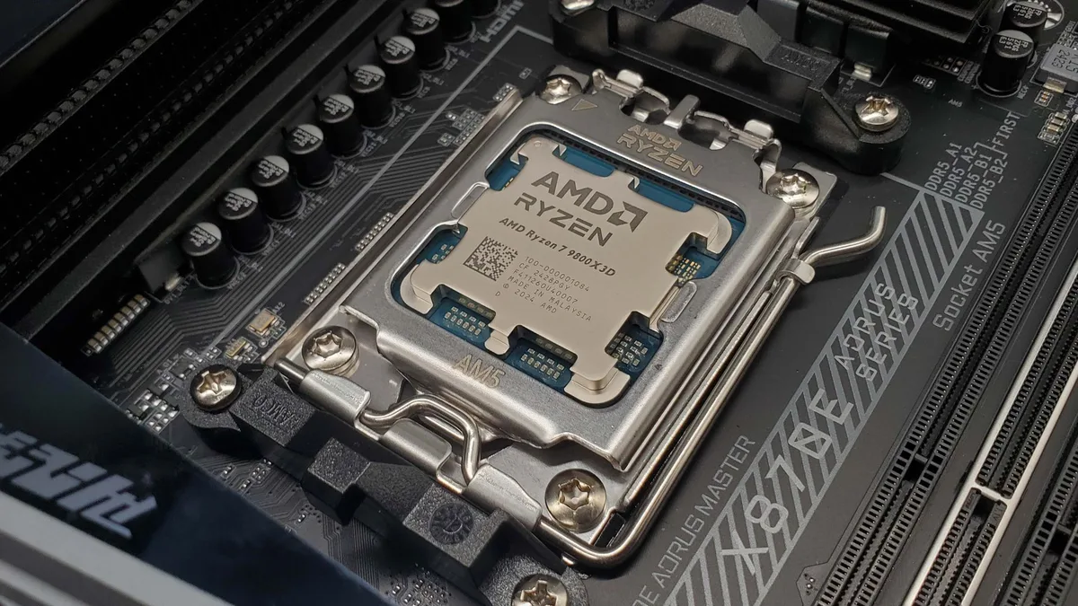
Whenever AMD's server architects pull back the curtain on their latest data center silicon, they are simultaneously handing PC builders the exact blueprint for the desktop gaming processors arriving months down the road. Alongside its enterprise showcase for the EPYC 9006 "Venice" family and the EPYC 9006 LP "Verano" platform engineered to cut server DDR5 usage by 50%, the Santa Clara chipmaker released a deep architectural breakdown of its high-performance Zen 6 compute cores. Between a historic jump to 12 cores per chiplet (CCD) on 2nm silicon, a specialized 3D V-Cache variant scaling to 144MB of L3 cache per CCD, and an average 27% IPC uplift, the specifications point to a massive generational leap for future AMD Ryzen desktop processors ("Olympic Ridge") on Socket AM5.
Breaking the 8-Core Ceiling: 12 Zen 6 Cores and 48MB of Native L3 Cache on a Single 2nm CCD
From the debut of Zen 3 in 2020 all the way through today's Zen 5 Ryzen 9000 lineup, AMD's standard high-performance Core Complex Dies (CCDs) have remained locked at a maximum layout of 8 physical cores sharing 32MB of L3 cache. With Zen 6, fabricated on TSMC's cutting-edge N2P (2nm-class) process node, AMD finally shatters that physical ceiling by packing 12 full-performance cores onto a single CCD (distinct from the dense cloud-focused Zen 6c chiplets, which pack up to 32 compact cores per die).
Because AMD preserves its foundational allocation of 4MB of native L3 cache per core, the shared local cache pool inside a single standard CCD rises proportionally from 32MB on Zen 5 to 48MB on Zen 6 (+50%). For PC gamers, this structural shift solves one of the longest-standing latency compromises in the Ryzen desktop stack.
On current desktop processors, a 12-core chip (such as a Ryzen 9 7900X or 9900X) has to split its compute engines across two separate 6-core chiplets. The moment a game engine stretches past 6 cores or passes threads between chiplets over the Infinity Fabric interconnect, cross-CCD latency penalties eat into frame rates. With Zen 6, a future 12-core / 24-thread Ryzen processor can live entirely on a single silicon die, allowing all 12 cores to tap into the exact same 48MB L3 cache pool with zero inter-chiplet overhead, while dual-CCD flagship Ryzen 9 models can scale up to 24 cores and 48 threads. Even better, AMD has already committed to supporting Socket AM5 past 2029, giving current motherboard owners a direct drop-in upgrade path.
Venice-X and Next-Gen 3D V-Cache: Setting the Stage for 144MB Single-CCD Gaming Chips
The second major revelation comes straight from the spec sheet of AMD's specialized EPYC "Venice-X" (9006X series) lineup, built for memory-bound technical computing, computational fluid dynamics, and electronic design automation. Venice-X pairs eight standard 12-core Zen 6 CCDs (96 cores total) with vertically stacked 3D V-Cache fused via advanced 3D Hybrid Bonding, reaching a staggering 1,152MB (1.15GB) of total L3 cache per socket while sustaining peak boost clocks up to 5.30 GHz.
The per-chiplet math for future Ryzen X3D gaming processors is crystal clear: dividing 1,152MB across eight chiplets means each 12-core Zen 6 CCD carries 144MB of total L3 cache. Since 48MB of that resides natively on the 2nm base die, the stacked 3D V-Cache slice jumps from 64MB (on Zen 4 and Zen 5) to 96MB per CCD (+50%). Brought over to a single-CCD Ryzen X3D gaming chip, players are looking at 12 unified cores backed by 144MB of L3 cache, up from 8 cores and 96MB on today's reigning Ryzen 7 9800X3D, completely bypassing dual-CCD Windows scheduling headaches.
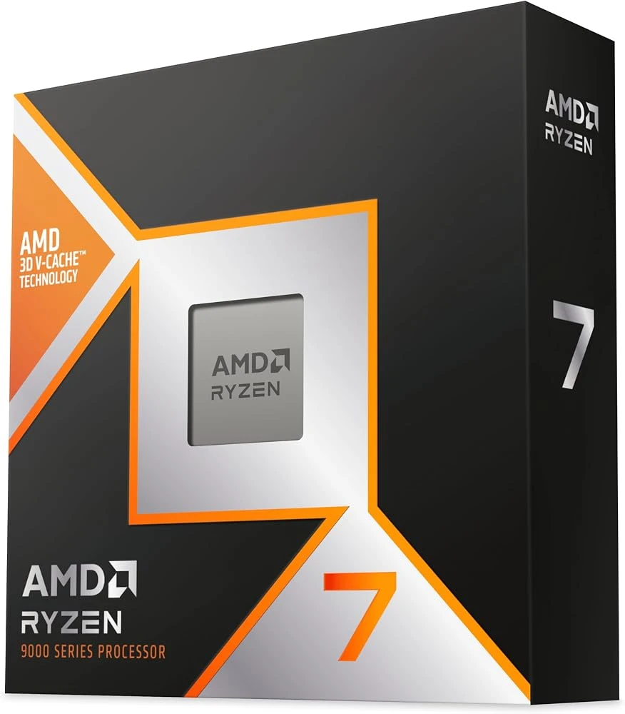
AMD Ryzen 7 9800X3D (Socket AM5, 96MB 3D V-Cache Gaming CPU)
- 8-core / 16-thread Zen 5 architecture with 96MB total L3 3D V-Cache
- Up to 5.2 GHz boost clock and fully unlocked for overclocking
- Socket AM5 platform ready for future Ryzen Zen 6 upgrades

352-Entry Register File, 640-Entry ROB, and +27% IPC: Feeding the Execution Engine
When Zen 5 launched on desktop, hardware analysts noted that while AMD had significantly widened the front-end instruction decoder, internal data pathways sometimes lacked the bandwidth needed to keep every execution unit fully fed during gaming workloads. With Zen 6, AMD aggressively expanded the core's internal plumbing to eliminate register starvation and bandwidth bottlenecks:
| Architectural Metric | AMD Zen 5 (Ryzen 9000) | AMD Zen 6 (Venice / Next-Gen Ryzen) | Generational Gain |
|---|---|---|---|
| CCD Manufacturing Node | TSMC N4P (4nm-class) | TSMC N2P (2nm-class) | Full node shrink |
| Cores per Standard CCD | 8 cores / 16 threads | 12 cores / 24 threads | +50% cores per chiplet |
| Native L3 Cache per CCD | 32MB (4MB per core) | 48MB (4MB per core) | +50% base L3 cache |
| Stacked 3D V-Cache per CCD | +64MB (96MB total L3) | +96MB (144MB total L3) | +50% stacked L3 cache |
| Integer Physical Register File (PRF) | 240 entries | 352 entries | +46.7% capacity |
| Reorder Buffer (ROB) | 448 entries | 640 entries | +42.8% deeper window |
| Op-Cache & Internal Link | 12-bit-wide connection | 6.75K entries / 18-bit-wide link | +50% op-cache bandwidth |
| Vector & AI Engine (FPU) | 2 VNNI INT8 pipes | 4 VNNI INT8 pipes + native AVX-512 FP16 | 2x INT8 throughput |
Scaling the Integer Physical Register File (PRF) from 240 up to 352 entries and expanding the Reorder Buffer (ROB) from 448 to 640 entries allows each Zen 6 core to track vastly more instructions in flight close to the execution units. At the same time, the operation cache grows to roughly 6.75K entries while widening its internal data connection from 12-bit to 18-bit, delivering a 50% surge in raw op-cache bandwidth. Paired with deeper load/store queues, enlarged schedulers, and native full-rate AVX-512 FP16 execution, these refinements combine for an average 27% IPC improvement over Zen 5 at iso-frequency.
My Take on the Spec Sheet
Looking closely at AMD's internal block diagrams for Zen 6, what stands out to me is how directly the engineering team targeted the exact bottlenecks that held non-X3D Zen 5 chips back in gaming. On Ryzen 9000, the wider front-end sometimes acted like a six-lane highway funneling into a two-lane tunnel whenever register entries or op-cache bandwidth ran dry. Jumping to a 352-entry integer register file, a 640-entry ROB, and an 18-bit op-cache link removes that internal choke point completely.
For Socket AM5 gamers, however, the real game-changer is the move to a 12-core TSMC N2P CCD paired with 144MB of total L3 cache in its 3D V-Cache configuration. Having 12 high-frequency cores sharing a single 144MB L3 pool without ever crossing the Infinity Fabric or relying on Windows core-parking drivers to manage a second chiplet is going to set a ferocious bar for 1% Low frametime stability. We obviously have not tested desktop Zen 6 silicon in our lab yet, so as soon as consumer engineering samples are ready, our test bench doors are wide open if AMD wants to put them head-to-head against the 9800X3D.

PC hardware enthusiast and competitive gamer, Arthur 'Heimdall' splits his time between France and the UK working in enterprise B2B software solutions. A business school graduate passionate about component benchmarking, he has been building, modding, and tuning PCs since childhood, optimizing every thermal degree and millisecond of display latency. An avid gamer across Assassin's Creed and sandbox titles, he forged his alliance with Grimtag and Chaya during late-night World of Warcraft raids before joining Pro-Gamer.