1nm (A10) Fab in Tainan and 2nm Mass Production: Taiwan's Science Minister Tips TSMC's Next-Gen GPU and CPU Manufacturing Hub
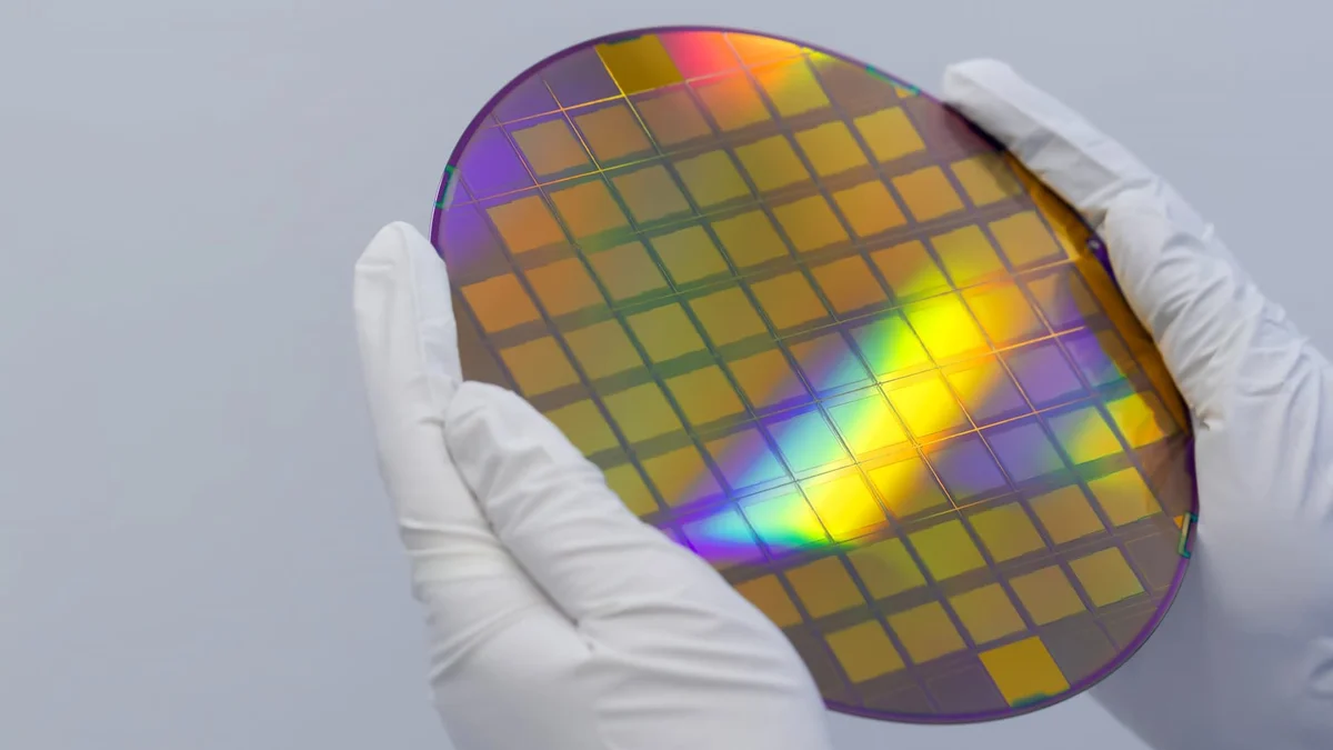
Even as the global semiconductor industry is only beginning its transition to Gate-All-Around (GAA) nanosheet transistors, Taiwan is already locking in the physical infrastructure for the 2030 silicon era. Speaking at the IEEE Asia Solid-State Circuits Conference (A-SSCC) in Tainan, Cheng-Wen Wu, Minister of Taiwan's National Science and Technology Council (NSTC), outlined government plans to establish a next-generation 1-nanometer (A10 node) manufacturing park within the Southern Taiwan Science Park (STSP) ecosystem.
Tainan and Shalun Starting in 2027: Land, Water, and Power for 1nm Lithography
Addressing semiconductor engineers at the IEEE conference, Minister Wu revealed that the Taiwanese government is preparing to develop a dedicated new park zone under the Tainan Science Park administration tailored specifically for 1-nanometer process technologies. While Wu did not explicitly name the foundry on stage, only one domestic chipmaker operates at the bleeding edge of sub-2nm lithography: TSMC, whose internal infrastructure plans point directly to Tainan's Shalun district as the home of its multi-phase Fab 25 giga-fab complex.
According to the timeline shared by the NSTC chief, site development for the new Tainan hub is scheduled to begin in 2027. With TSMC's 2-nanometer (N2) node now entering mass production, Wu emphasized that pushing forward to 1nm requires far more than cleanroom transistor breakthroughs: it demands early cross-government coordination on land acquisition, ultra-pure water supply, and high-capacity power grids.
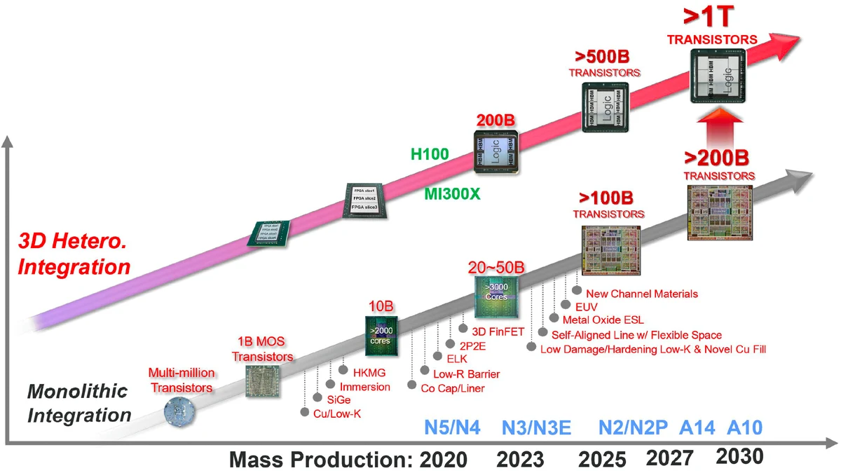
From 2nm to 1.4nm (A14) and 1nm (A10): The Silicon Roadmap to 2030
Before 1-nanometer wafers ever roll off Tainan production lines, TSMC is focused on delivering its intermediate Angstrom-era milestone: the A14 (1.4-nanometer) process node. Officially slated for high-volume manufacturing in 2028, industry supply-chain schedules indicate that A14 risk production could commence as early as the second half of 2027 to qualify fab tooling ahead of mass ramp. That relentless cadence keeps intense pressure on competing foundries, especially as Intel bets heavily on 14A High-NA EUV lithography and manufacturing scale to close the gap with TSMC.
Alongside site selection in southern Taiwan, TSMC is also tackling the atomic-level physics required to push past the 1nm barrier. Working in partnership with researchers at National Yang Ming Chiao Tung University (NYCU), the foundry recently achieved a critical breakthrough in transistor surface engineering designed to curb quantum leakage and resistance in sub-1-nanometer channel structures.
| TSMC Process Node | Lithography Class | Production Timeline | Expected Hardware Targets (CPU / GPU) |
|---|---|---|---|
| N3E / N3P | 3nm-class (FinFET) | Mature volume (2024 - 2026) | Current-gen GPUs, high-density CPU chiplets |
| N2 / N2P | 2nm-class (GAA Nanosheet) | Active mass production (2026 - 2027) | Next-gen Ryzen Zen 6 CPUs and AI accelerators |
| A14 | 1.4nm-class (14 Angstroms) | Risk H2 2027 / Volume in 2028 | AMD Zen 7 CPUs and RDNA 5+ GPUs (2028 - 2029) |
| A10 | 1nm-class (10 Angstroms) | Tainan park dev in 2027 / Target ~2030 | 1-trillion-transistor 3D packages, post-2030 GPUs & CPUs |
Silicon Photonics, Robotics, and What It Means for Gaming Hardware
Beyond wafer lithography, Minister Wu highlighted two enabling technologies during his IEEE A-SSCC address: optical communications and advanced robotics. He noted that optical interconnects (silicon photonics) must evolve beyond enterprise server racks to serve broader computing applications, replacing power-hungry copper traces with high-bandwidth light pathways. At the same time, expanding Taiwan's robotics supply chain will allow domestic metal, polymer, and advanced materials producers to transition into high-value cleanroom and automation ecosystems.
For PC gamers, TSMC's southern Taiwan expansion lays the groundwork for the architectures that will succeed late-decade Radeon, GeForce, and Ryzen lineups. Even as Intel prepares its 18A-P Nova Lake desktop CPUs for CES 2027 to challenge Ryzen X3D, today's top gaming desktops already rely heavily on TSMC silicon pairing Zen 5 cores with second-generation 3D V-Cache technology.
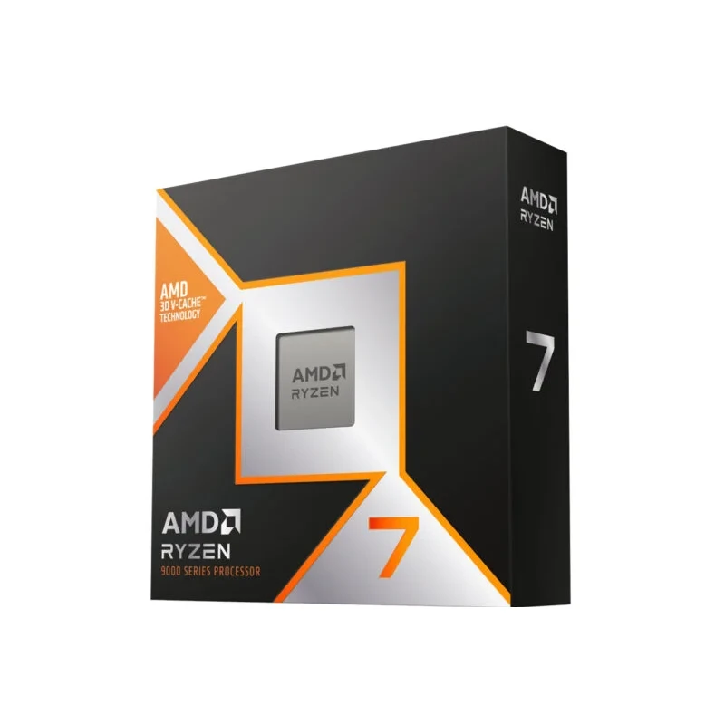
AMD Ryzen 7 9800X3D Gaming Processor (8 Cores / 16 Threads, 2nd-Gen 3D V-Cache, Socket AM5)
- TSMC-built Zen 5 architecture with 96MB of 2nd-Gen 3D V-Cache L3 memory
- 8 cores and 16 threads boosting up to 5.2 GHz
- Future-ready Socket AM5 platform with DDR5 and PCIe 5.0 support
- Outstanding gaming efficiency per watt (120W TDP)
Check Availability AMD Ryzen 7 9800X3D on Amazon→
My Take on the Spec Sheet
Looking at Minister Cheng-Wen Wu's Tainan disclosures from a PC builder's perspective highlights both an engineering marvel and a looming pricing challenge. On the technical side, laying the groundwork in 2027 for a 1nm (A10) manufacturing hub while pushing optical interconnects outside data-center racks shows how seriously TSMC is tackling the thermal density and copper resistance walls that currently cap GPU and CPU clock speeds. At the same time, the economics of sub-2nm lithography are staggering: between next-generation EUV scanners, massive ultra-pure water infrastructure, and soaring 300mm wafer prices from N2 to A14 and A10, leading-edge silicon is becoming exponentially more expensive to fab. The real test for gamers will be how AMD and NVIDIA balance die sizes and chiplet packaging so future graphics cards and desktop processors remain within reach of mainstream builds. Because these sub-nanometer nodes are still at the industrial planning stage, we are evaluating this trajectory from official roadmap disclosures rather than physical silicon on our bench; if the engineering teams at AMD, NVIDIA, or TSMC would like to send over their upcoming processor and GPU architectures as soon as hardware samples roll out for full thermal and power-efficiency testing in our lab, our test bench is wide open. We have not yet had a physical unit on our desk—if the manufacturer's team would like to send over a review sample so we can put it through our full real-world testing protocol, our lab doors are wide open.

PC hardware enthusiast and competitive gamer, Arthur 'Heimdall' splits his time between France and the UK working in enterprise B2B software solutions. A business school graduate passionate about component benchmarking, he has been building, modding, and tuning PCs since childhood, optimizing every thermal degree and millisecond of display latency. An avid gamer across Assassin's Creed and sandbox titles, he forged his alliance with Grimtag and Chaya during late-night World of Warcraft raids before joining Pro-Gamer.