Intel Xeon 7 "Diamond Rapids" Server Processor Unveiled in Shenzhen: 256 Panther Cove-X Units on 18A-P and 1.28 GB L3 Cache
Packing up to 256 high-performance cores on the Intel 18A-P process node, 1.28 GB of L3 cache, and a massive substrate sitting on 9,324 contact pads, Intel used the Tencent Global Digital Ecosystem Summit in Shenzhen to publicly display the first physical silicon samples of its next-generation Xeon 7 "Diamond Rapids" server processor. Scheduled for a 2027 commercial launch at the heart of the Oak Stream platform, this heavy-duty chip built for agentic AI infrastructure will go head-to-head against AMD's formidable EPYC 9006 "Venice" processors powered by Zen 6.
A Massive Silicon Package on the LGA 9324 Socket Shown Front and Back in Shenzhen
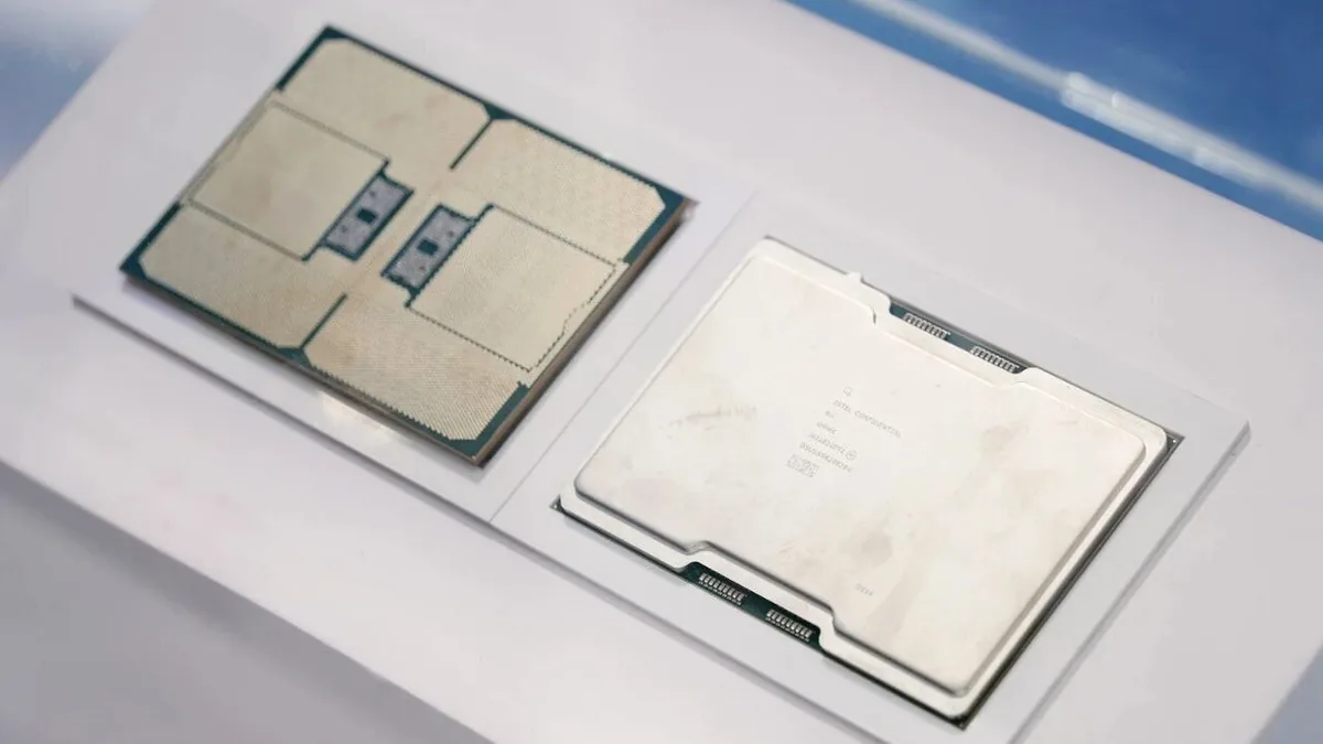
Inside the display cases at the Shenzhen technology summit, two engineering samples stamped INTEL CONFIDENTIAL offered the first real-world look at the physical footprint of Diamond Rapids. One unit showcased a newly sculpted integrated heat spreader (IHS) with asymmetrical side cutouts, while the flipped unit alongside it exposed the four massive gold contact pad banks of the LGA 9324 socket framing two central rows of capacitors.
That mechanical footprint is engineered to deliver and cool a thermal design power (TDP) scaling up to 650W on a single socket. This giant interface matches the upcoming generation of Oak Stream server boards, including the recently unveiled ASRock Rack DMRD16-2L+ E-ATX motherboard capable of housing 4 TB of DDR5 around the exact same LGA 9324 socket.
256 Panther Cove-X Cores on 18A-P, 1.28 GB Cache, and 1.6 TB/s Memory Bandwidth
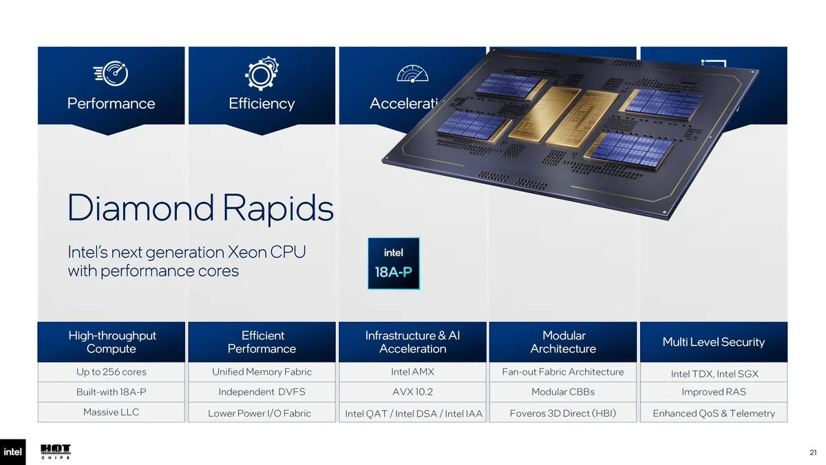
Beneath its metal heat spreader, the flagship Intel Xeon 7 configuration brings together up to 256 P-Cores built on the Panther Cove-X microarchitecture, distributed across 16 modular compute chiplets (Compute Building Blocks). In a major architectural shift, Intel has dropped Simultaneous Multithreading (SMT / Hyper-Threading) on these server cores, delivering a strict 256-core / 256-thread layout to maximize per-core throughput, power efficiency, and predictable tail latency.
On the manufacturing side, Diamond Rapids serves as the inaugural data center processor built on the performance-enhanced Intel 18A-P node (combining RibbonFET Gate-All-Around transistors with PowerVia backside power delivery), laying the high-volume silicon foundation that precedes Intel's future desktop roadmap leading up to Nova Lake and 2028's Razor Lake-S. The processor's I/O tiles are fabricated on the Intel 3 node and stitched to the compute chiplets via Foveros 3D Direct (HBI) hybrid bonding.
| Technical Feature | Intel Xeon 7 "Diamond Rapids" Specification |
|---|---|
| Platform & Socket | Intel Oak Stream / LGA 9324 Socket (9,324 contact pads) |
| Cores & Microarchitecture | Up to 256 Panther Cove-X P-Cores (256 threads, no SMT) across 16 compute tiles |
| Process Nodes & Packaging | Intel 18A-P compute tiles + Intel 3 I/O tiles (Foveros 3D Direct HBI) |
| L3 Cache (LLC) | Up to 1.28 GB of Last-Level Cache |
| Memory Subsystem | 16-channel DDR5: RDIMM up to 8,000 MT/s and MRDIMM up to 12,800 MT/s (~1.6 TB/s) |
| I/O & AI Acceleration | 128 PCIe Gen 6 lanes, CXL support, Intel AMX and AVX 10.2 (512-bit) |
| Thermal Design Power (TDP) | Up to 650W |
To keep all 256 cores fed without memory starvation, Intel paired the compute array with a massive 1.28 GB L3 cache (Last-Level Cache) and a 16-channel DDR5 memory controller. Supporting multiplexed MRDIMM modules running at up to 12,800 MT/s (alongside standard DDR5 RDIMMs at 8,000 MT/s), the platform reaches up to 1.6 TB/s of memory bandwidth and provides 128 PCIe Gen 6 lanes.
Intel Core Ultra 7 265K (20 Cores, up to 5.5 GHz)
- 20-core hybrid architecture (8 P-Cores + 12 E-Cores) boosting up to 5.5 GHz on LGA 1851
- Native support for high-speed DDR5 memory and 20 PCIe 5.0 lanes
- Integrated NPU hardware acceleration and optimized thermal efficiency for gaming and heavy workloads
Check Availability Intel Core Ultra and Xeon Processor Availability on Amazon→
Tencent Cloud Co-Development, Agentic AI, and the Showdown With AMD EPYC Zen 6
During the Shenzhen keynote, Intel and Tencent Cloud also announced the joint development of next-generation CVM (Cloud Virtual Machine) instances powered by Diamond Rapids, pitching the chip as a purpose-built backbone for agentic AI infrastructure. By combining built-in Intel AMX matrix engines with AVX 10.2 instructions, Intel claims small-model LLM inference speedups of 1.3x to 3.4x compared to traditional AVX-512 execution on idle CPU cores.
While Diamond Rapids prepares for its 2027 rollout, Tencent Cloud has already deployed Intel's current Xeon 6+ "Clearwater Forest-AP" processors (featuring up to 288 E-Cores on 18A) across its production cloud. According to telemetry shared on stage, Xeon 6+ nodes sustain more than 350 concurrent sandboxes with an average creation latency of 200 milliseconds (a 1.46x improvement over prior test beds), enabling Tencent's Cube Sandbox platform to spin up over 100,000 isolated sandboxes within minutes.

Even with those specs on the table, Intel faces a steep uphill battle in 2027. Diamond Rapids will arrive against already-established AMD EPYC 9006 "Venice" processors built on the Zen 6 architecture, which also scale up to 256 cores with 12,800 MT/s MRDIMM support while boasting a massive 27% IPC uplift over Zen 5, ahead of Intel's subsequent Coral Rapids generation targeted for 2028.
My Take on the Spec Sheet
Looking at the underside of that LGA 9324 package and its 1.28 GB L3 cache pool makes Intel's engineering priorities crystal clear: ditching Hyper-Threading across all 256 Panther Cove-X cores lets every single physical thread tap into a massive 1.6 TB/s memory pipe and dedicated cache without sibling contention. That is exactly what high-density virtualization and CPU-side LLM token generation crave when memory latency is the primary bottleneck. Still, taming 650W per socket while going up against AMD's Zen 6 EPYC lineup and its 27% IPC jump is a brutal thermal and architectural test. This initial breakdown is based on the official specifications and silicon samples shown in Shenzhen; we still need to verify real-world 18A-P power curves and sustained all-core clocks under heavy rack loads. If Intel's team is reading this, our test bench has space ready whenever validation hardware or workstation derivatives are available for a full thermal and telemetry pass.

PC hardware enthusiast and competitive gamer, Arthur 'Heimdall' splits his time between France and the UK working in enterprise B2B software solutions. A business school graduate passionate about component benchmarking, he has been building, modding, and tuning PCs since childhood, optimizing every thermal degree and millisecond of display latency. An avid gamer across Assassin's Creed and sandbox titles, he forged his alliance with Grimtag and Chaya during late-night World of Warcraft raids before joining Pro-Gamer.