Samsung's New 8LPU+ Chip Process Could Power a Cheaper Nintendo Switch 2 Lite With 12% Higher Performance
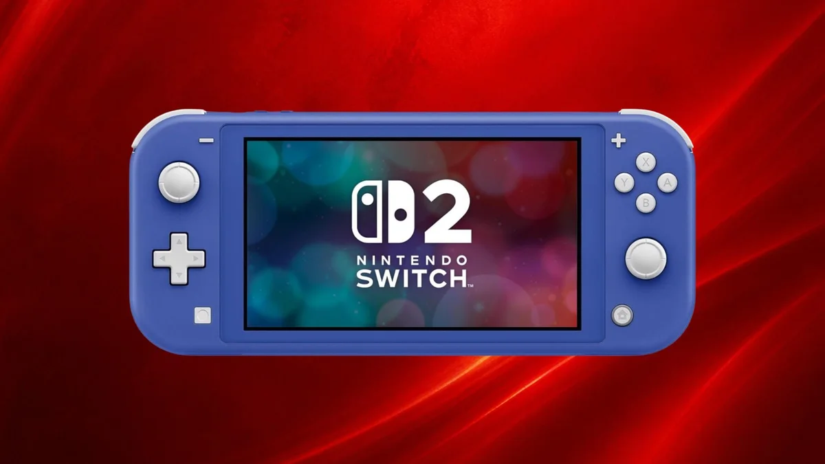
As surging component prices continue to squeeze console hardware margins, a realistic manufacturing path toward a more affordable portable version of Nintendo's latest hybrid system is taking shape. According to South Korean industry publication The Electronic Times and the technical program for the upcoming IEDM 2026 (IEEE International Electron Devices Meeting) spotted by analyst Nintendo Patents Watch, Samsung Foundry will introduce a second-generation 8-nanometer process platform called 8LPU+ before the end of December. Offering higher density, lower power draw, and far lower wafer costs than EUV nodes, the refined silicon platform stands out as a prime candidate for the custom Nvidia T239 processor inside a future Nintendo Switch 2 Lite.
Inside Samsung's 8LPU+ Node: 12% Performance Gain, 15% Less Power, and 8% Smaller Logic Area
Eight years after developing its initial 8LPP process in 2017 and introducing the first 8LPU iteration in 2018, Samsung Electronics is extending its mature 8nm family with the 8LPU+ platform, set to be formally detailed at IEDM 2026 in December. Compared directly against standard 8LPU silicon, the upgraded node brings measurable improvements across every key metric for handheld hardware:
- 12% higher performance at equivalent power envelopes;
- 15% lower power consumption at matching clock speeds;
- 8% smaller logic area across the core compute die;
- Roughly 10% smaller input/output (I/O) area by integrating 3.3V planar I/O devices directly into the 8LPU FinFET process;
- Significantly reduced standby current leakage through ultra-low-leakage SRAM (ULL-SRAM), high-threshold-voltage devices (cHVT), and embedded magnetoresistive RAM (eMRAM) boasting a 0.017 μm² bit-cell area and ~20 Mb/mm² density.
The biggest advantage of 8LPU+ lies in its manufacturing economics. While cutting-edge 5nm, 4nm, and 2nm nodes rely on extreme ultraviolet (EUV) lithography machines built exclusively by ASML at a cost of hundreds of billions of won per unit, Samsung's 8nm family uses argon fluoride immersion deep ultraviolet (DUV) equipment. Because those DUV production lines have already undergone full financial depreciation and accumulated years of predictable yield data, wafer fabrication costs remain substantially lower.
Why the Nintendo Switch 2's Custom Nvidia T239 SoC Is a Natural Fit
Although Samsung is heavily marketing 8LPU+ toward automotive zone control units (ZCUs), robotics, and edge AI microcontrollers, an industry official quoted by The Electronic Times noted that "existing 8nm customers in Samsung Foundry's ecosystem" are prime candidates for the transition. In consumer electronics, the highest-volume 8nm chip at Samsung Foundry is the custom Nvidia T239 SoC powering the Nintendo Switch 2, which utilizes a custom Ampere-based 8N derivative closely related to 8LPP.
At a time when Samsung is locking nearly 80% of its memory capacity for AI customers, soaring LPDDR5X RAM and NAND flash storage prices have made hardware cost reductions exceptionally difficult. Moving the T239 to 8LPU+ instead of funding an expensive redesign on a 4nm EUV node would give Nintendo three major advantages: more chips per wafer thanks to the 8% logic shrink and 10% I/O reduction, 100% native software compatibility with the entire Switch 2 library without changing the underlying SoC architecture, and a 15% power reduction that allows for a smaller battery and lighter cooling assembly.
Surging R&D Spending and the Original Switch Lite's European Exit in February 2027
Broader corporate signals from Kyoto also point toward a dedicated entry-level handheld in the pipeline. As tracked by Nintendo Patents Watch, Nintendo's Research and Development (R&D) expenditures climbed sharply during the fiscal year ended March 2026,matching historical spending spikes that preceded earlier hardware form-factor revisions.
Nintendo has already started iterating on its assembly lines to comply with European Union right-to-repair mandates, even though a recent teardown of the revised Switch 2 model confirmed it retains the same LCD panel alongside its easier-to-swap battery tray. More importantly, Nintendo is scheduled to discontinue the original Nintendo Switch Lite in Europe starting in February 2027, leaving a clear gap at the budget end of its portable lineup. Whether a future Switch 2 Lite features a smaller LCD screen with integrated non-detachable controls and no TV dock output, or simply trims manufacturing costs to hit a lower price point much like the Nintendo 2DS did during the 3DS era, Samsung's 8LPU+ node provides a timely foundation.
My Perspective: Why Mature 8nm DUV Silicon Is Nintendo's Smartest Play Against the Memory Crunch
From a hardware engineering standpoint, it is easy to wish for a 4nm or 3nm die shrink whenever a handheld revision is discussed. In the current semiconductor market, however, paying top dollar for ASML EUV lithography wafers while LPDDR5X memory contract prices are climbing would defeat the entire purpose of a budget Lite console.
Staying on Samsung's fully depreciated DUV lines with 8LPU+ is the kind of pragmatic engineering choice Nintendo has favored for decades. Shaving 15% off power draw and nearly 10% off the combined logic and I/O footprint gives hardware designers just enough thermal and electrical headroom to shrink the battery pack, simplify the heatsink, and build a single-piece handheld shell without breaking game compatibility or inflating the bill of materials. With the original Switch Lite bowing out of Europe in February 2027, all eyes will be on Samsung's December IEDM presentation.

Based on the outskirts of New York City, Chaya 'Chayane' spent five years studying software engineering in Montreal before returning to her home state. A Full-Stack developer and Deep Learning AI architecture researcher, she explores neural networks and algorithmic optimization while engineering data pipelines for Retrocharting and Gamescharting alongside Grimtag. A gamer for over 20 years and an avid collector of Nintendo history and The Legend of Zelda, she explored World of Warcraft's Azeroth before bringing her deep technical background to video game analysis.