GeForce RTX 5070 With a 378 mm² GB203 Die vs. GB205: A 43% Larger Chip With Zero Extra FPS
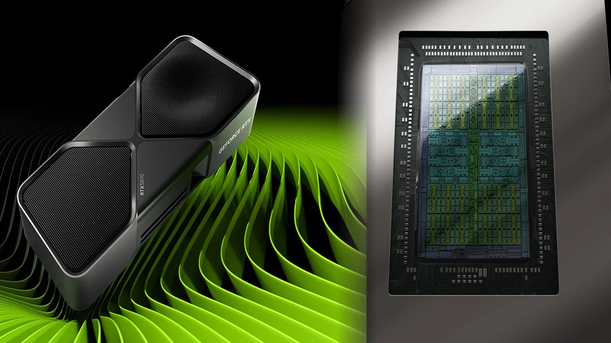
Behind the scenes of modern graphics card manufacturing, two retail boxes carrying the exact same model name do not always hide the same piece of silicon underneath their heatsinks. Just as Nvidia continues to withhold 415W GB203-450 design schematics for the upcoming GeForce RTX 5080 24GB from board partners, industry attention in early November 2026 has returned to a secondary hardware revision of the GeForce RTX 5070 built around the larger GB203 die instead of the baseline GB205-300 chip. Originally tipped by hardware leaker hongxing2020 in early September and still unconfirmed officially by Nvidia, this die substitution raises an obvious question for PC builders: does landing a higher-tier GPU die inside an RTX 5070 translate into extra gaming performance? From an engineering standpoint, the answer is a definitive no.
GB203 vs. GB205-300: A 43% Larger Die Heavily Cut Down by Laser
In its standard commercial configuration, the GeForce RTX 5070 is powered by the GB205-300-A1 silicon fabricated on the TSMC 4N process node. Measuring 263 mm² and packing 31.1 billion transistors, the baseline GB205 die utilizes its full physical layout: 48 Streaming Multiprocessors (SMs) totaling 6,144 CUDA cores, 192 fifth-generation Tensor Cores, 48 fourth-generation RT Cores, and a 192-bit memory interface paired with 12GB of GDDR7 VRAM (28 Gbps, delivering 672 GB/s of bandwidth) within a 250W Total Graphics Power (TGP) envelope.
By contrast, the GB203 die is the substantially larger silicon Nvidia natively reserves for upper-tier enthusiasts cards, namely the GeForce RTX 5070 Ti and GeForce RTX 5080. Physically, the footprint gap is massive: the GB203 chip spans 378 mm² (+43.7% larger than GB205) and houses 45.6 billion transistors (+46.6%), with a full physical ceiling of 84 SMs (10,752 CUDA cores) and a 256-bit memory bus.
| Technical Specification | GeForce RTX 5070 (Baseline GB205) | GeForce RTX 5070 (GB203 Variant) | Full GB203 Silicon (RTX 5080) |
|---|---|---|---|
| Silicon Die (TSMC 4N) | GB205-300 (100% enabled) | GB203 (~57% enabled) | GB203-400 (100% enabled) |
| Die Area | 263 mm² | 378 mm² | 378 mm² |
| Transistor Count | 31.1 billion | 45.6 billion (~43% disabled) | 45.6 billion |
| Compute Units (SM / CUDA) | 48 SMs / 6,144 CUDA Cores | 48 SMs / 6,144 CUDA Cores | 84 SMs / 10,752 CUDA Cores |
| Video Memory (VRAM) | 12GB GDDR7 (192-bit, 672 GB/s) | 12GB GDDR7 (192-bit, 672 GB/s) | 16GB GDDR7 (256-bit, 960 GB/s) |
| Total Graphics Power (TGP) | 250W | 250W | 360W |
To repurpose a GB203 chip into a GeForce RTX 5070, Nvidia severely trims the silicon: 36 out of 84 SMs are disabled (cutting roughly 43% of its compute blocks) and two of its eight 32-bit memory controllers are shut off to narrow the bus from 256-bit down to 192-bit. Because the active shader count (6,144 CUDA cores), memory buffer (12GB GDDR7), reference clock targets (~2,325 MHz base and ~2,512 MHz boost), and 250W power limit remain strictly locked to baseline specifications, 1440p and 4K frame rates remain virtually indistinguishable from a standard GB205 card.
The Economics of Die Harvesting: Salvaging Imperfect GB203 Silicon
If gamers gain zero extra frame rate, why would Nvidia mount a more expensive 378 mm² chip onto a lower-tier graphics card? The answer lies in semiconductor yield management, commonly referred to as binning or die harvesting. As TSMC wafers come off the production line, not every GB203 die meets the strict electrical or defect thresholds required for an RTX 5080 or RTX 5070 Ti. Some chips suffer minor manufacturing defects across specific compute clusters or memory channels, while others fail to sustain top boost clocks at target voltage curves.
Rather than scrapping those partially defective GB203 dies entirely, Nvidia fuses off the faulty sections and ships the silicon as a GeForce RTX 5070. This harvesting strategy is already established across the Blackwell lineup: select GeForce RTX 5060 production batches similarly utilize a cut-down GB205 chip in place of the native GB206 die. For Add-in-Card (AIC) partners such as ASUS, MSI, Gigabyte, PNY, and Zotac, mixing in harvested GB203 dies helps stabilize GPU supply amidst ongoing wafer and memory constraints.
Thermals, vBIOS Mods, and Cooler Compatibility: What Actually Changes for Buyers
Even though in-game performance stays flat, swapping a 263 mm² die for a 378 mm² chip introduces physical nuances that PC builders and modders should keep in mind. From a thermal standpoint, dissipating 250W across a wider silicon footprint alters heat flux density and leaves large sections of inactive dark silicon beneath the cooler coldplate or vapor chamber. However, because board design, VRM power stages, and factory fan curves vary across custom AIC models, a larger die does not automatically guarantee lower operating temperatures or quieter acoustics.
Where the distinction truly matters is hardware compatibility and low-level firmware. A GB203-based GeForce RTX 5070 requires its own PCI Device ID, modified PCB routing, and a dedicated vBIOS firmware supported by Nvidia GeForce drivers. As a result, cross-flashing a GB205 vBIOS onto a GB203 card (or vice versa) will fail, and any hope of unlocking disabled CUDA cores or memory channels via software mods is blocked by physical laser fusing on the die. Custom watercooling builders must also verify the exact GPU revision in GPU-Z before ordering a full-cover waterblock, as BGA package tolerances and surrounding SMD component layouts can differ between PCB revisions.
On the retail front, while GDDR7 memory inflation is already pressuring GPU street prices ahead of Black Friday on November 27, custom GeForce RTX 5070 12GB models currently trade in early November 2026 starting around $578 to $650 on Amazon US for dual- and triple-fan baseline designs (such as ASUS Prime and MSI Ventus/Shadow), while premium factory-overclocked editions climb between $700 and $900+, with no retail label separating GB205 and GB203 batches.
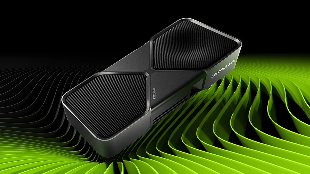
Nvidia GeForce RTX 5070 (12GB GDDR7)
- Nvidia Blackwell Architecture (6,144 CUDA Cores, 48 SMs)
- 12GB GDDR7 VRAM on a 192-bit Bus (672 GB/s)
- Full DLSS 4 / DLSS 5 and Reflex 2 Support at 250W TGP
My Bench Take
Do not fall into the trap of hunting down a GB203-based GeForce RTX 5070 expecting a hidden "silicon lottery" performance boost. Because Nvidia laser-locks the disabled SMs and memory controllers at the hardware level, both the 263 mm² GB205-300 and the harvested 378 mm² GB203 deliver the exact same 6,144 CUDA cores, 192-bit memory bus, and 672 GB/s bandwidth. If you are shopping for an RTX 5070 this month, pick your card based on cooler build quality and actual street price rather than paying a single dollar extra for a die swap designed purely to maximize Nvidia's wafer yields.
That said, how a 378 mm² die with over 40% dark silicon distributes 250W of heat under sustained load is a fascinating thermal question that deserves real-world instrumentation. We have not yet had this GB203 revision of the GeForce RTX 5070 on our test bench: if Nvidia or any of its AIC board partners would like to send over a retail sample once these units hit shelves so we can measure HotSpot deltas, transient power draw, and overclocking headroom side-by-side against the original GB205 model, our test lab is wide open.

PC hardware enthusiast and competitive gamer, Arthur 'Heimdall' splits his time between France and the UK working in enterprise B2B software solutions. A business school graduate passionate about component benchmarking, he has been building, modding, and tuning PCs since childhood, optimizing every thermal degree and millisecond of display latency. An avid gamer across Assassin's Creed and sandbox titles, he forged his alliance with Grimtag and Chaya during late-night World of Warcraft raids before joining Pro-Gamer.