Capacitorless Z2RAM Memory: How Pat Gelsinger-Backed Nagare Labs Targets SRAM Speed at DRAM Density
It is the single biggest physical bottleneck in modern computer architecture: SRAM cache is blazingly fast but devours an unsustainable amount of silicon die area below 3 nm, while conventional DRAM offers high bit density at the cost of high latency and constant power-hungry refreshes. Stepping out of stealth with a $5 million seed round led by Playground Global and former Intel CEO Pat Gelsinger, Georgia Tech spinout Nagare Labs has unveiled Z2RAM, a capacitorless memory architecture designed to deliver SRAM-class speed at DRAM-level density.
A Capacitorless 2T Oxide-Semiconductor Cell Stacked Directly on Logic Dies
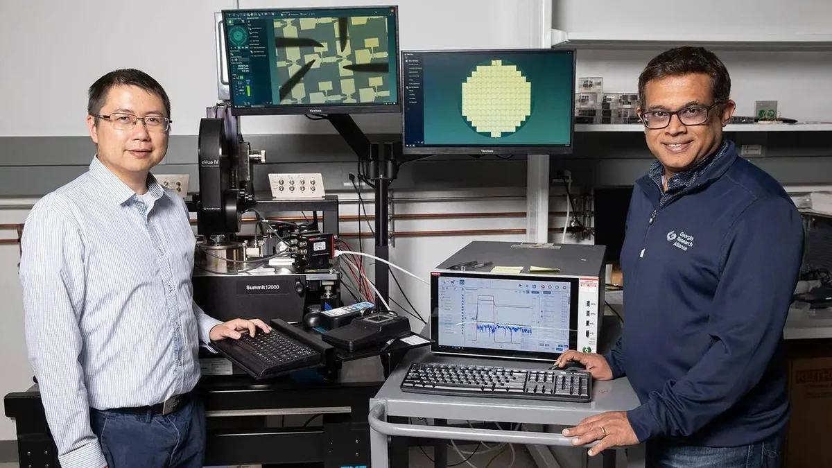
Developed out of semiconductor research at the Georgia Institute of Technology by co-founders and professors Suman Datta (CEO) and Shimeng Yu (CTO), Z2RAM (Zero-Ionization, Zero-Swing RAM) eliminates the bulky physical capacitor found in traditional 1T1C DRAM cells. Instead, it uses a capacitorless two-transistor (2T) gain-cell design built from oxide semiconductors, storing the data charge directly within the gate capacitance of the second transistor.
Because these oxide-semiconductor layers can be deposited at low temperatures during Back-End-Of-Line (BEOL) processing on standard 300 mm wafers, Z2RAM can be grown and vertically stacked in 3D directly on top of CPU, GPU, or AI compute dies without requiring expensive interposers or side-by-side HBM packaging. For PC builders who have seen firsthand how vertical cache transforms gaming frame times,most notably with AMD's Ryzen 7 5800X3D and its 96 MB of vertically stacked 3D V-Cache,the prospect of monolithic, ultra-dense 3D cache is immediately compelling.
| Technical Metric | 2 nm High-Density SRAM / 1T1C DRAM | Nagare Labs Z2RAM Architecture |
|---|---|---|
| Cell Structure | 6-Transistor (SRAM) or 1T1C with Capacitor (DRAM) | Capacitorless 2T Gain Cell (Oxide Semiconductor) |
| Bit Density | Severe SRAM scaling wall at 2 nm nodes | Over 5x the bit density of 2 nm SRAM in Gen-1 3D stacks |
| Access Speed & Read Power | High DRAM latency / High SRAM static power draw | 14x faster access than DRAM at one-third the read energy of SRAM |
| Data Retention at 85°C | DRAM requires refresh cycles every 32 ms to 64 ms | Over 300 seconds at 85°C demonstrated in published lab testing |

AMD Ryzen 7 5800X3D (Socket AM4)
- 8 Cores / 16 Threads Zen 3 (3.4 GHz Base / 4.5 GHz Boost)
- 96MB L3 3D V-Cache Vertically Stacked Memory
- Socket AM4 with DDR4 Support (105W TDP)
- Ultimate Drop-In Gaming Upgrade Without Motherboard Swap
Over 300 Seconds of Retention at 85°C and 5x the Density of 2 nm SRAM
Historically, gain-cell memory prototypes have struggled with rapid charge leakage, losing stored bits in microseconds under high thermal loads and requiring constant refresh cycles. By leveraging the ultra-low off-state leakage current of oxide semiconductors, the latest published cells from Datta and Yu's research groups achieved data retention exceeding 300 seconds at 85°C,roughly four orders of magnitude longer than conventional DRAM refresh intervals.
For its first-generation multi-layer stack, Nagare Labs projects more than 5x the bit density of 2 nm high-density SRAM (scaling toward 10x in future iterations), 14x faster access speeds than standard DRAM, and a 67% reduction in read energy compared to SRAM. While traditional memory giants execute Micron's roadmap toward DDR6 and 1-delta DRAM nodes, Pat Gelsinger,who joins Nagare Labs' board of directors alongside his role as General Partner at Playground Global,views monolithic BEOL 3D memory stacking as a foundational shift to break the memory wall across next-generation processors.

My Take on the Spec Sheet
If you want to understand why flagship CPUs and GPUs keep getting more expensive to manufacture, look no further than SRAM scaling. Ever since TSMC crossed below the 5 nm threshold, standard 6-transistor SRAM cells have barely shrunk at all, forcing AMD and NVIDIA to rely on costly hybrid-bonded cache dies or massive memory buses. Replacing six silicon transistors with a two-transistor oxide cell that holds its charge for over five minutes at 85°C while packing 5x the cache density directly on top of a compute die is every chip architect's dream scenario. That said, we need to keep our feet on the ground: this is currently an early-stage laboratory technology backed by a $5 million seed round. Turning a Georgia Tech probe-station breakthrough into high-yield, defect-free 300 mm mass production will take years of fab qualification, and we will be watching closely as Nagare Labs delivers its first commercial silicon prototypes.

PC hardware enthusiast and competitive gamer, Arthur 'Heimdall' splits his time between France and the UK working in enterprise B2B software solutions. A business school graduate passionate about component benchmarking, he has been building, modding, and tuning PCs since childhood, optimizing every thermal degree and millisecond of display latency. An avid gamer across Assassin's Creed and sandbox titles, he forged his alliance with Grimtag and Chaya during late-night World of Warcraft raids before joining Pro-Gamer.