1-Delta DRAM, 400-Layer G11 NAND, and High-NA EUV: Inside Micron's Memory Roadmap Through 2030

With global memory fabs running at maximum capacity to feed artificial intelligence accelerators, Micron Technology has officially unveiled its multi-year DRAM and NAND roadmap stretching through 2030. Led by President and Chief Technology and Products Officer Scott DeBoer, the US memory giant outlined a bold architectural pivot: scrapping long-researched 4F² DRAM cells entirely, launching its 1-delta (1δ) DRAM node and 400-plus-layer G11 3D NAND in the second half of 2027, adopting advanced wafer bonding, preparing High-NA EUV lithography, and bringing back custom silicon with co-designed cHBM4E and vertically stacked vHBM.
1-Delta DRAM, Wafer Bonding, and High-NA EUV: Why Micron Axed 4F² Cells on the Road to 3D DRAM
One of the biggest surprises from Micron's technology briefing is its decision to pull the plug on future 4F² DRAM cell architectures after two decades of internal research. While competitors such as Samsung, SK hynix, and CXMT are actively pursuing 4F² layouts, Scott DeBoer explained that the supposed density advantages of 4F² are largely a myth because capacitor pitch at the angstrom scale remains the true physical bottleneck. Instead, Micron is extending its proven 6F² planar cell architecture across four more generations while developing two generations of vertically stacked memory, labeled 3D1 and 3D2 (3D DRAM), in parallel.
Building on its current high-volume 1-gamma (1γ) node, which marked the company's first use of standard EUV lithography, Micron will bring its next-generation 1-delta (1δ) process into mass production in the second half of 2027 at its US fabrication facilities. The 1δ node targets a mid-20% bit density improvement over 1γ by pairing advanced high-k metal gate (HKMG) CMOS transistors with new materials and angstrom-level process control. This node will underpin future DDR6 memory (targeting twice the bandwidth of DDR5), LPDDR6 (co-optimized with Meta to cut power consumption by 35% compared to LPDDR5), next-generation graphics memory, and HBM5.
Looking beyond 2027, Micron's planar roadmap continues with the 1-epsilon (1ε) node, which introduces wafer bonding to DRAM manufacturing so logic structures and memory cells can be fabricated on separate wafers before being bonded together. Following 1ε, the zeta-angstrom (ζÅ) node will introduce High-NA EUV lithography similar to next-generation 1.4nm foundry roadmaps around the 2030 timeframe, succeeded by the pathfinding eta-angstrom (ηÅ) generation alongside 1st and 2nd Generation 3D CMOS logic designed to deliver a 10x peripheral performance leap between 2020 and 2030.
Custom HBM4E and Vertical vHBM: How AI Co-Design Reshapes GPUs and Consumer PC Memory Supply
Micron also confirmed a major resurgence of custom silicon across its high-bandwidth memory portfolio. Starting with Custom HBM4E (cHBM4E) and continuing into Custom HBM5E, Micron is co-designing the memory's logic base die directly with AI processor customers. Manufactured on advanced external foundry CMOS nodes, these custom base dies offload circuitry that would traditionally sit inside the GPU or ASIC itself, freeing up compute die area while optimizing memory interface width and power efficiency.
Even more ambitious is Micron's upcoming vertical HBM (vHBM) and vertical Edge Inference Memory (vEIM). Rather than placing HBM stacks beside a GPU on a silicon interposer, vHBM stacks memory directly on top of the compute processor using hybrid bonding and integrated heat spreaders. First-generation vEIM targets an impressive 2 TB/s of HBM4-class bandwidth while consuming less than 1 picojoule per bit (< 1 pJ/bit) of data transfer energy. As surging data center demand pushes semiconductor revenues to historic highs, this deep co-allocation of wafer capacity toward custom AI memory explains why mainstream DDR5 kits continue to command elevated retail prices across North America.
400-Layer G11 3D NAND: Skipping G10 to Double Flash Density in Late 2027
On the storage front, Micron revealed that it is bypassing a 10th-generation node entirely, leaping straight from its current 276-layer G9 (N160) 3D NAND to 11th-generation G11 (N170) 3D NAND in the second half of 2027. By adopting wafer-on-wafer bonding (fabricating the memory cell arrays on one wafer and the CMOS peripheral and I/O circuitry on another before bonding them) and pushing past 400 active layers, G11 will double bit density from roughly 21 Gb/mm² on G9 to 42 Gb/mm² for 3D TLC flash.
Performance and efficiency gains for upcoming PCIe 5.0 and PCIe 6.0 SSDs are equally substantial: G11 boosts per-die I/O transfer speeds by 50% from 3,600 MT/s to approximately 5,400 MT/s, while cutting data transfer energy consumption by more than 25% per bit. Alongside conventional enterprise SSDs scaling up to 512 TB, Micron is developing two specialized AI storage tiers: High-IOPS AI NAND (using small-block SLC architectures to deliver 25 million to 100 million IOPS) and High-Bandwidth AI NAND stacked via TSVs on a logic base die close to compute engines. For PC builders upgrading their rigs today, Micron's flagship consumer performance remains anchored by the Crucial T705 2TB PCIe 5.0 NVMe SSD, currently retailing around $366.00 USD.
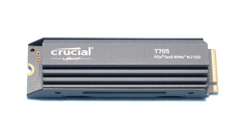
Crucial T705 2TB PCIe Gen5 NVMe M.2 SSD
- PCIe 5.0 NVMe M.2 (up to 14,500 MB/s)
- Micron 3D TLC NAND Flash
- Integrated aluminum & copper heatsink
- Microsoft DirectStorage ready
Micron DRAM and 3D NAND Technology Roadmap Summary (2026 to 2030)
| Technology / Node | Key Architecture and Innovations | Production Target | Target Products and PC Hardware Impact |
|---|---|---|---|
| 1-gamma (1γ) DRAM | 6F² cells, Micron's first EUV DRAM process | In high-volume manufacturing (2026) | High-speed DDR5, LPDDR5X, and HBM3E |
| 1-delta (1δ) DRAM | 6F² cells, advanced HKMG CMOS, mid-20% bit density gain | 2H 2027 (US manufacturing) | DDR6 (2x DDR5 bandwidth), LPDDR6 (-35% power), GDDR, HBM5 |
| 1-epsilon (1ε) and ζÅ / ηÅ | Wafer bonding (1ε), High-NA EUV (ζÅ), and 3D CMOS | Late decade / 2030+ | Continued 6F² planar scaling without 4F² compromises |
| 3D DRAM (3D1 and 3D2) | Vertical DRAM cell stacking | Parallel development | Long-term successor to conventional planar DRAM |
| cHBM4E, vHBM and vEIM | Custom logic base dies and direct vertical stacking on XPUs | 2027 to 2030 | 2 TB/s at < 1 pJ/bit (vEIM), AI accelerators and future halo GPUs |
| G11 (N170) 3D NAND | 400+ layers, wafer-on-wafer bonding, 42 Gb/mm² TLC density | 2H 2027 | 5,400 MT/s I/O (+50%), -25% energy/bit for PCIe 5.0/6.0 SSDs |
My Tech Bench
Looking closely at Scott DeBoer's roadmap, two very different takeaways stand out for PC builders. On the storage side, Micron skipping G10 to bring 400-plus-layer G11 3D NAND with wafer-on-wafer bonding to market in the second half of 2027 is fantastic news. Doubling TLC bit density to 42 Gb/mm² while trimming energy per bit by 25% will directly drive down the cost per gigabyte of high-capacity 4TB and 8TB PCIe 5.0 NVMe drives, while helping them run noticeably cooler under sustained gaming loads.
On the system memory side, however, the resurgence of custom silicon through cHBM4E and direct-stacked vHBM sends a clear warning for your wallet. Because hyperscalers are now co-designing base dies with Micron years in advance, and every HBM wafer consumes roughly three times the silicon area of standard desktop memory, consumer DDR5 supply will remain tight well into 2027. If you are planning an AM5 or next-gen platform build, locking in your storage and memory upgrades when you spot a solid retail price remains the smartest play rather than waiting on 1-delta and DDR6 to arrive late next year.

PC hardware enthusiast and competitive gamer, Arthur 'Heimdall' splits his time between France and the UK working in enterprise B2B software solutions. A business school graduate passionate about component benchmarking, he has been building, modding, and tuning PCs since childhood, optimizing every thermal degree and millisecond of display latency. An avid gamer across Assassin's Creed and sandbox titles, he forged his alliance with Grimtag and Chaya during late-night World of Warcraft raids before joining Pro-Gamer.