
3.9 GHz on the Radeon RX 9070 GRE (+40% Clock Speed): How DirectX 9 Pushes AMD’s RDNA 4 Silicon to the Limit
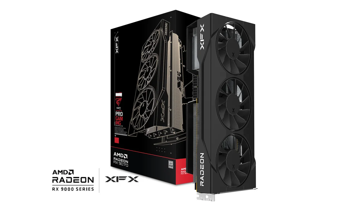
Pushing a retail graphics card more than 1,110 MHz beyond its official Boost specification without a single drop of liquid nitrogen or any physical hardware modification is enough to make any silicon enthusiast look twice. Yet that is the exact milestone recorded on an AMD Radeon RX 9070 GRE, whose reported core clock hit 3.9 GHz (3,900 MHz) during an experiment conducted by hardware developer and overclocker ShrimpBrime. Behind that headline figure lies a clever software trick: a custom-built DirectX 9 rendering workload specifically designed to sidestep the power, current, and thermal walls of AMD's RDNA 4 architecture.
A Stock XFX Radeon RX 9070 GRE Swift Pushed to 3,900 MHz on Air Cooling
Unlike traditional world-record overclocking runs that rely on liquid nitrogen pots chilled to -196°C and heavily modified circuit boards, this demonstration was carried out on an off-the-shelf retail card. The experiment used a standard XFX Swift AMD Radeon RX 9070 GRE Triple Fan Gaming Edition running on its original air cooler (featuring three 100mm double ball-bearing fans) and its stock factory VBIOS, with no physical shunt mods applied to its dual 8-pin PCIe power connectors.
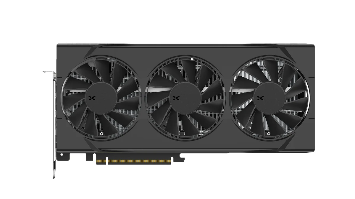
Under the hood, the Radeon RX 9070 GRE is powered by the Navi 48 XL die fabricated on TSMC's 4nm process (spanning 357 mm² with 53.9 billion transistors). This cut-down RDNA 4 configuration packs 48 Compute Units (3,072 Stream Processors), 48 third-generation Ray Accelerators, and 96 second-generation AI matrix cores, paired with 12 GB of GDDR6 memory across a 192-bit bus delivering 432 GB/s of bandwidth. At a time when the graphics card market is already bracing for another AMD Radeon RX 9000 GPU and GDDR6 memory price increase, this 220W TBP card ships from the factory with a 2,220 MHz Game Clock and an official Boost rating of up to 2,790 MHz (2.79 GHz).
By reaching a reported core clock (GFXCLK) of 3,900 MHz, the Navi 48 die achieved a theoretical jump of +39.8% over its official Boost target. Even before hitting the 3.9 GHz peak with custom tuning utilities, the developer noted that clock speeds around 3.85 GHz (3,850 MHz) could be reproduced repeatedly using the native tuning sliders inside AMD Software: Adrenalin Edition.
Why a 4.19-Million-Triangle DirectX 9 Loop Unleashes RDNA 4 Clock Scaling
To understand how a GPU rated just under 2.8 GHz can climb to 3.9 GHz on air, you have to look closely at the workload fed to the silicon. Rather than launching a demanding modern game, ShrimpBrime wrote two custom utilities tailored for AMD Radeon hardware: R-Team OC (RTOC), a high-frequency telemetry monitoring and tuning tool, and GPU Frequency Generator, a lightweight rendering application built on the legacy DirectX 9 API.
| Technical Parameter | Official AMD Factory Spec | DirectX 9 Experiment (ShrimpBrime) |
|---|---|---|
| Card Model & Silicon | Radeon RX 9070 GRE (Navi 48 XL / 4nm RDNA 4) | XFX Swift RX 9070 GRE (Stock VBIOS & Air Cooler) |
| Compute Units / VRAM | 48 CUs (3,072 SPs) / 12 GB GDDR6 (192-bit, 432 GB/s) | Unmodified Retail Hardware (No Shunt Mod) |
| GPU Frequency (Game / Boost) | 2,220 MHz (Game) / Up to 2,790 MHz (Boost) | 3,900 MHz (3.9 GHz) Reported GFXCLK (+39.8%) |
| Applied Workload | Modern DirectX 12 / Vulkan Games (220W TBP) | GPU Frequency Generator DX9 (4.19M triangles/frame) |
| Real-World Stability | Fully Stable Under Heavy 3D Load | Proof-of-Concept Only (Driver Crashed After Capture) |
Specifically, the DirectX 9 tool renders a stripped-down geometry scene consisting of 2,048 triangles per draw call and 2,048 draw calls per frame, which works out to roughly 4.19 million triangles per frame. For a modern architecture like RDNA 4, processing a basic triangle loop without complex pixel shaders, heavy texture fetches, or matrix math places virtually zero stress on the execution engines.
When a modern AAA game runs under DirectX 12 or leverages next-generation rendering pipelines like AMD's upcoming FSR Diamond with Multi-Frame Generation and Ray Reconstruction, all 3,072 stream processors, caches, and the GDDR6 memory subsystem draw heavy current at the exact same time. That simultaneous load immediately hits the 220W power limit and forces the dynamic boost controller to dial back clock speeds. Conversely, the featherlight DirectX 9 triangle scene draws minimal wattage and keeps die temperatures low, leaving massive electrical and thermal headroom that allows the boost algorithm to push GFXCLK all the way to 3.9 GHz.
The developer behind the test was quick to point out the practical caveats of the experiment. First, the reported GFXCLK metric reflects the driver-polled target clock rather than a guaranteed sustained effective frequency across all shader arrays. Second, even under this trivial DirectX 9 loop, the graphics driver eventually crashed and recovered shortly after the 3.9 GHz telemetry screenshots were captured.
My Take on the Spec Sheet: The 3.9 GHz Mirage Versus the DirectX 12 Wall
From a pure silicon engineering standpoint, I appreciate what ShrimpBrime accomplished here by isolating the behavior of Navi 48's clock generator. Seeing 4nm TSMC silicon report 3,900 MHz on a standard triple-fan air cooler shows that the front-end clock domains of the RDNA 4 architecture can switch at remarkable frequencies when they are not starved for power.
That said, we need to separate telemetry experiments from real-world gaming performance. Spinning 4.19 million unshaded triangles in DirectX 9 has nothing in common with sustaining a stable 1440p framerate in a heavy DirectX 12 title. As soon as all 48 Compute Units and the 192-bit GDDR6 bus are hammered by complex shader execution and ray tracing, transient current spikes and VRM thermal impedance kick in immediately. In actual gaming workloads, trying to squeeze even an extra 200 to 300 MHz out of a Radeon RX 9070 GRE hits an exponential voltage-to-frequency wall that ruins power efficiency long before delivering meaningful extra frames on screen.
In the interest of full transparency, we have not yet had the Radeon RX 9070 GRE on our own test bench to map its real-world voltage curves and thermal behavior under load. If AMD or board partners such as XFX, Sapphire, and PowerColor would like to send a Radeon RX 9070 GRE review sample over to our lab, we would gladly put it through our full DirectX 12 torture suite at 1440p to see what this Navi 48 XL chip can truly sustain in modern games.

PC hardware enthusiast and competitive gamer, Arthur 'Heimdall' splits his time between France and the UK working in enterprise B2B software solutions. A business school graduate passionate about component benchmarking, he has been building, modding, and tuning PCs since childhood, optimizing every thermal degree and millisecond of display latency. An avid gamer across Assassin's Creed and sandbox titles, he forged his alliance with Grimtag and Chaya during late-night World of Warcraft raids before joining Pro-Gamer.