12.8 to 14.4 GT/s Data Rates, 96-Bit Bus, and 74mm Modules: JEDEC Previews the DDR6 Memory Standard
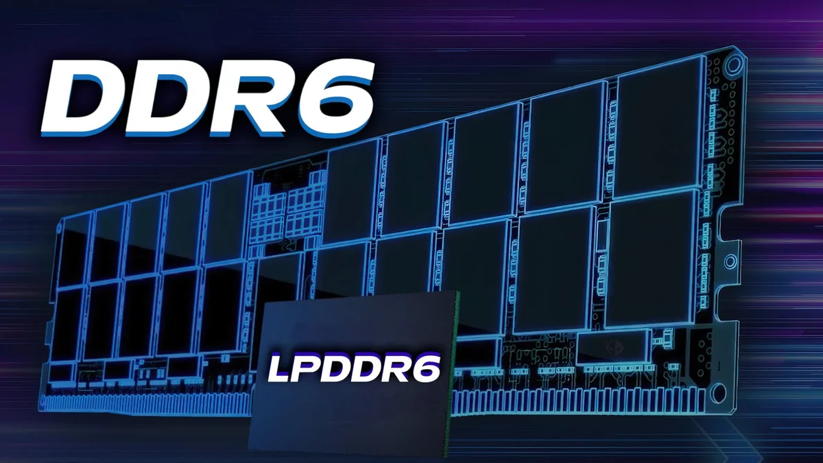
The JEDEC Solid State Technology Association, the microelectronics standards body representing over 400 member companies including Samsung, SK Hynix, Micron, Intel, and AMD, has published its first official technical preview of the upcoming DDR6 DRAM standard. Developed within the JC-42 Committee for Solid State Memories, DDR6 overhauls traditional system memory by expanding the data bus width by 50%, doubling internal bank availability, and cutting physical module length by roughly 44% to serve next-generation client PCs, workstations, and AI data centers.
Starting at 12.8 GT/s With a Roadmap to 14.4 GT/s and a 96 DQ Data Bus
On the performance front, JEDEC confirms that DDR6 will push well past DDR5's official 9.2 GT/s server ceiling. Initial DDR6 RDIMM implementations are scheduled to launch at a baseline transfer rate of 12.8 GT/s (12,800 MT/s), with an early roadmap scaling up to 14.4 GT/s (14,400 MT/s) and beyond as DRAM fabrication nodes mature.
Even more impactful than the raw frequency jump is the redesigned channel interface. While DDR5 relies on a 64-bit module width, DDR6 expands the data bus from 64 to 96 DQ, representing a 50% increase in data lines. According to Christopher Cox, Chair of JEDEC's JC-42 Committee for Solid State Memories, the combination of higher data rates and the wider 96 DQ bus delivers more than a 50% bandwidth increase right at introduction compared to DDR5.
To keep that wider interface fed without sacrificing efficiency, DDR6 organizes memory access into a pseudo-channel architecture paired with flexible system-level error-correcting code (ECC) options. Furthermore, JEDEC is doubling the internal bank count (2X bank count) and introducing upgraded refresh mechanisms to maximize bus utilization across high-speed, high-capacity configurations.
44% Shorter 74mm Modules and UDIMM, RDIMM, and CAMM Form Factors
One of the most visible changes in the DDR6 preview involves the physical footprint of the memory sticks themselves. Standard desktop and server DIMMs have measured roughly 133mm in length across multiple generations of DDR memory. With DDR6, JEDEC specifies a compact 74mm module length, making the new layout approximately 44% shorter than a 133mm DDR5 stick.
Shrinking the module outline solves a fundamental electrical hurdle. At data rates between 12.8 GT/s and 14.4 GT/s, long copper trace paths introduce signal reflection and impedance challenges between the DRAM packages and the processor's integrated memory controller. Moving to a 74mm footprint tightens trace routing, improves signal integrity, and frees up valuable board real estate for dense server and desktop motherboard layouts.
JEDEC notes that the DDR6 specification is being defined across multiple form factors, explicitly encompassing RDIMM for servers, UDIMM for desktop client systems, and CAMM modules to balance signal performance, thermal dissipation, power, and upgradability.
Up to 128Gb DRAM Dies, VSS-Terminated I/O, and Market Outlook
For capacity scaling, the DDR6 blueprint adds support for monolithic DRAM die densities of up to 128Gb (16GB per individual chip), alongside architectural optimizations for advanced die stacking within a single package footprint. Power efficiency is also addressed by switching from traditional VDDQ termination to VSS-terminated I/O and implementing data-center-oriented low-power states to improve performance per watt.
- Transfer Rates: Starts at 12.8 GT/s (12,800 MT/s) at launch, scaling to 14.4 GT/s (14,400 MT/s) and higher.
- Bus Architecture: Expands by 50% from 64 DQ to 96 DQ with pseudo-channels and 2X internal bank count.
- Bandwidth Uplift: Over 50% higher memory bandwidth at introduction versus DDR5.
- Die Density: Supports up to 128Gb (16GB) DRAM dies with die-stacking optimizations.
- Physical Footprint: Narrower 74mm module length (44% shorter than 133mm DDR5) across RDIMM, UDIMM, and CAMM designs.
As JEDEC Board of Directors Chairman Mian Quddus emphasized, these parameters represent the active development preview currently under review by member firms prior to final publication. The announcement arrives at a pivotal moment for PC builders, who are already grappling with tight DDR5 RAM inventory and elevated pricing projected to stretch through 2027 as memory foundries prioritize AI server contracts.
Unlike consumer NAND flash wafer spot prices that recently dropped 20% to 32%, DRAM fabrication remains heavily contested, meaning DDR6 will first deploy in enterprise and AI inference servers before transitioning to next-generation consumer desktop platforms later in the decade.
My Test Bench
Looking closely at JEDEC's architectural outline, the real breakthrough here goes beyond the headline 14.4 GT/s speed target: it is the pairing of a 96 DQ pseudo-channel bus with a 74mm physical module length. On current DDR5 desktop motherboards, pushing past 8,000 MT/s across standard 133mm DIMM slots quickly runs into signal integrity walls. By trimming 44% off the module length, adopting VSS-terminated I/O, and baking in native support for both compact UDIMMs and CAMM layouts, the JC-42 committee is directly addressing the physical trace bottlenecks that limit high-frequency RAM today. While DDR5 will remain the backbone of gaming PCs for the next several years, DDR6 lays a far cleaner electrical foundation for future desktop sockets.

PC hardware enthusiast and competitive gamer, Arthur 'Heimdall' splits his time between France and the UK working in enterprise B2B software solutions. A business school graduate passionate about component benchmarking, he has been building, modding, and tuning PCs since childhood, optimizing every thermal degree and millisecond of display latency. An avid gamer across Assassin's Creed and sandbox titles, he forged his alliance with Grimtag and Chaya during late-night World of Warcraft raids before joining Pro-Gamer.